Need help with gain of a BJT amplifier, circuit.

Status
Not open for further replies.

MrAl

Joined Jun 17, 2014
13,765
Yes - that`s correct.
The AC analysis contains three basic steps:
* Finding the signal input resistance r,in at the base node (incl. R1 and R2); this necessary because of the source resistor RG.
* Computing the gain (referenced to the base node) using the formula A1=gm(RC||RL)/[1+gm(RE1)]
*
Computing the total gain A=A1[r,in/(r,in+RG)]
Well for now i am just interested in computing the gain.

So you find 're' and then use that in the AC analysis?
Or you use use some formula as above? If so, where did you get the formula?
 

LvW

Joined Jun 13, 2013
2,035
As I have told you, I was using the mentioned formulas.(without "re" but with "gm=1/re").
Do you want me to derive the formula?
In principle, it is the classical formula for a gain with negative feedback:
Closed loop gain Acl=Aol/(1+loop gain) with Aol=-gm(RC||RL)
 

MrAl

Joined Jun 17, 2014
13,765
As I have told you, I was using the mentioned formulas.(without "re" but with "gm=1/re").
Do you want me to derive the formula?
In principle, it is the classical formula for a gain with negative feedback:
Closed loop gain Acl=Aol/(1+loop gain) with Aol=-gm(RC||RL)
Hello again,

Well if you just throw formulas out then if someone gets a different result then you wont be able to tell what is wrong. All you will be able to conclude is that either the formula is wrong or if you assume it is right then the other guy is wrong, but you wont really have any proof.
If you look at Jony's circuit and replies you will see we can trace every step that he did, and each step involves a specific circuit and assumption. If one of the assumptions is "This formula is correct A=K*J*M+4" then we cant trace the origin of that formula, or at least you should try to do that.
It's ok of course if you opt out of this, but if you want to get to the bottom of it then you might find out what circuit is being used and how that formula came about. I say this because you got a different result too.
I was trying to get everyone on the same page, or at least explain why we have some small differences.
It is important for you to understand i am not knocking the formula, i just need more basic information about this.
So yes maybe you should derive the formula.
 

LvW

Joined Jun 13, 2013
2,035
Hello again,

Well if you just throw formulas out then if someone gets a different result then you wont be able to tell what is wrong. All you will be able to conclude is that either the formula is wrong or if you assume it is right then the other guy is wrong, but you wont really have any proof.
...............................
So yes maybe you should derive the formula.
MrAl, Hello again.

I am afraid that I must disappoint you - let me explain:
I am an engineer and I know that (a) no formulas are correct by 100% and (b) that all parts values enter the formulas with errors (tolerances, uncertainties). More that, taking this background into consideration it makes no sense to compute voltages, currents and gain values up to an accuracy of 0.01% or better.
I like to remember you that we have assumed: VBE=0.65 V and VT=26mV and beta=B=300 - knowing that no value meets reality.
That`s OK because we do not have better (more accurate) values.
However, do you really think - having these uncertainties in mind - that in my calculation I was using the value of 15k||68k=12.289k ?
Of course, for further calaculations I have used (as far as I remember) R1||R2=12.3k.
And the same applies to some other "odd" values.
As another example, I have computed the DC emitter voltage with VE=1.0797 V.
Of course, for further calculations I have used a value of 1.08 V.

From the engineering point of you it would be stupid to enter values having a formal (mathematical) accuracy which is much much better than all the inaccuracies which are included in the whole system.
Having this in mind, I think the difference between Jonys results and my figures (app. 1.5%) is acceptable.
More than that, our results were confirmed by simulation. No surprise that Spice simulatins gave a somewhat smaller gain value (due to the finite BJT output resistance which was neglected during hand calculations and, of course better values for VBE and gm).
Hence, when someone has slightly other final results we really must not "conclude that either the formula is wrong or if you assume it is right then the other guy is wrong"
May I remind you that your result for the gain was A=11,109 (instead of app. 9.9).
Nothing is wrong - the small difference is caused by different accuracy properties during our calculation.
That`s quite normal for such (approximate) calculations.
May I again repeat that the analysis of such a circuit is a standard procedure to be found in many textbooks - and I think, therefore, it is really not necessary to "derive the formula" here in the forum.

Regards
LvW
 

MrAl

Joined Jun 17, 2014
13,765
MrAl, Hello again.

I am afraid that I must disappoint you - let me explain:
I am an engineer and I know that (a) no formulas are correct by 100% and (b) that all parts values enter the formulas with errors (tolerances, uncertainties). More that, taking this background into consideration it makes no sense to compute voltages, currents and gain values up to an accuracy of 0.01% or better.
I like to remember you that we have assumed: VBE=0.65 V and VT=26mV and beta=B=300 - knowing that no value meets reality.
That`s OK because we do not have better (more accurate) values.
However, do you really think - having these uncertainties in mind - that in my calculation I was using the value of 15k||68k=12.289k ?
Of course, for further calaculations I have used (as far as I remember) R1||R2=12.3k.
And the same applies to some other "odd" values.
As another example, I have computed the DC emitter voltage with VE=1.0797 V.
Of course, for further calculations I have used a value of 1.08 V.

From the engineering point of you it would be stupid to enter values having a formal (mathematical) accuracy which is much much better than all the inaccuracies which are included in the whole system.
Having this in mind, I think the difference between Jonys results and my figures (app. 1.5%) is acceptable.
More than that, our results were confirmed by simulation. No surprise that Spice simulatins gave a somewhat smaller gain value (due to the finite BJT output resistance which was neglected during hand calculations and, of course better values for VBE and gm).
Hence, when someone has slightly other final results we really must not "conclude that either the formula is wrong or if you assume it is right then the other guy is wrong"
May I remind you that your result for the gain was A=11,109 (instead of app. 9.9).
Nothing is wrong - the small difference is caused by different accuracy properties during our calculation.
That`s quite normal for such (approximate) calculations.
May I again repeat that the analysis of such a circuit is a standard procedure to be found in many textbooks - and I think, therefore, it is really not necessary to "derive the formula" here in the forum.

Regards
LvW

Hi,

Well ok, if you cant do it, that's ok man (just kidding here) :)

I agree almost completely, except i found a better result than 11.109 later when i found that all of you were using 're' as well. I had posted that in this thread.

But as far as 1 percent differences go, i was going to state that myself too so i agree with you totally there. But see i did not know that you used a rounded value of resistors until you stated that, so up to that point i had no explanation.

Now for me, sometimes i have to step into the role of the theoretician, and when i do that i look for EXACT results across the board. For my better result in this thread, i get nearly perfect results in my calculation AND in my simulation, and i can get even more exact by taking the time to enter a more exact value into the simulator, but as you i did not see it worthwhile when i know it will work because i do the same thing the simulator does in calculation. When i use symbolic results the results are always EXACT to any number of digits you wish to consider. Symbolically though they are already exact. That's the beauty of seeking symbolic solutions.

My goal was to explain the differences between all of our results, and i found something more interesting in doing so.
To explain i have to point out that when we have a change of topology (as we do in this circuit) the voltages and currents from the first structure to the second structure should be exactly the same (or very very nearly so). We should strive to produce the second topology such that before and after the change the voltages and currents remain the same, and the closer we get this the better we've done the job, if we cant get it exact.

To simplify how this theory works, if we have a voltage divider and calculate the output voltage and get a certain value for the current, then use that current to determine a third resistor, then insert that resistor in series with the other two resistors, we can not believe that the current will not decrease. Thus the change in topology caused a change in current which is not a good idea.
Now if it was a small value in relation to the others, then the degree of the skew of the result would depend on the ratio of the resistor values.
In many cases it is probably assumed small, but if not then all bets are off.

For this circuit at hand with the transistor, the difference between mine and say Jony's is probably because i did not assume to use a traditional method, but when ahead and tried to reduce any skew (as mentioned above) so as to get a more interesting result.
The result was that i got a more complicated formula for the resistance 're', but using that value, there is no change in the voltages or currents when i move from topology 1 to topology 2.
You may choose to ignore this and go with the more traditional solution, but if the values of the emitter resistor vs 're' are not widely different it could affect the results even more. I have not yet tried to determine any limits on this but i may in the past.

So in conclusion, it appears that your difference is because you rounded resistor values, but my difference is because i solved for perfect topologies in order to get a more accurate result, but i do admit that it may not always be necessary to do that.

If i get a chance i will try to illustrate this change in theory with a few circuits.
 

LvW

Joined Jun 13, 2013
2,035
.......................
To explain i have to point out that when we have a change of topology (as we do in this circuit) the voltages and currents from the first structure to the second structure should be exactly the same (or very very nearly so). We should strive to produce the second topology such that before and after the change the voltages and currents remain the same, and the closer we get this the better we've done the job, if we cant get it exact.
................................
Thus the change in topology caused a change in current which is not a good idea.

For this circuit at hand with the transistor, the difference between mine and say Jony's is probably because i did not assume to use a traditional method, but when ahead and tried to reduce any skew (as mentioned above) so as to get a more interesting result.
The result was that i got a more complicated formula for the resistance 're', but using that value, there is no change in the voltages or currents when i move from topology 1 to topology 2.
So in conclusion, it appears that your difference is because you rounded resistor values, but my difference is because i solved for perfect topologies in order to get a more accurate result, but i do admit that it may not always be necessary to do that.
If i get a chance i will try to illustrate this change in theory with a few circuits.
Well, thanks again for your detailed response.
However, there are still two questions from my side:
1.) "Change of topology": I must admit that I do not understand.
I know what you most probably mean (two different small-signal equivalent diagrams as shown by Jony) - however, both diagram do in fact represent the same set of equations. This can be proved! Hence, this cannot explain any differences.
More than that, you are mentioning a "perfect topology" for "more accurate results". May I ask, at which point and why is it "more accurat"?
Where is the improvement? How does this "perfect" topology look like?

2.) You are stating that you "got a more complicated formula for the resistance 're'.

This is interesting and I kindly ask you to give some more information about this point.
To me, the differential quantity "re" is nothing else than a new symbol for 1/gm where gm is the slope of the IC=f(VBE) characteristic - hence, the transconductance of the device.
(Calculating the slope of the exponential characteristic leads to gm=IC/Vt)
This is a definition - and I am curious to see how a your finding of the "re" value looks like.

Thank you, Regards
LvW
 
Last edited:

MrAl

Joined Jun 17, 2014
13,765
Well, thanks again for your detailed response.
However, there are still two questions from my side:
1.) "Change of topology": I must admit that I do not understand.
I know what you most probably mean (two different small-signal equivalent diagrams as shown by Jony) - however, both diagram do in fact represent the same set of equations. This can be proved! Hence, this cannot explain any differences.
More than that, you are mentioning a "perfect topology" for "more accurate results". May I ask, at which point and why is it "more accurat"?
Where is the improvement? How does this "perfect" topology look like?

2.) You are stating that you "got a more complicated formula for the resistance 're'.

This is interesting and I kindly ask you to give some more information about this point.
To me, the differential quantity "re" is nothing else than a new symbol for 1/gm where gm is the slope of the IC=f(VBE) characteristic - hence, the transconductance of the device.
(Calculating the slope of the exponential characteristic leads to gm=IC/Vt)
This is a definition - and I am curious to see how a your finding of the "re" value looks like.

Thank you, Regards
LvW
Hi again, and thanks again for the interesting reply and questions...

First, do you use any math software to do your calculations?
I ask because you can go back in the thread and find the formula i came up with for 're' and just copy that and paste into your math software and get a result right away without having to use a hand calculator.

I meant to get back here sooner with some circuits that illustrate the difference but i got involved in some government politics and some preparation for Christmas which is now right around the corner. That stuff takes some time.

The main idea is that when we solve some circuits we end up changing the topology of the circuit as we progress in the analysis. This is necessary and works very well. When we switch from one to the next however we have to make sure that all of the basic variables stay the same because if changing the topology alone changes anything important, then we skew the end result.
Is that was is happening here with the traditional analysis?
I think so, but the effect may be small, however i note this for the more general case.
Will it affect your analysis for this circuit with the assumed values and operating conditions?
Yes, but i dont think to a great extent, and you can see this by comparing my results to yours or Jony's.
So this is really mostly academic except when maybe the circuit setup happens to be such that the differences dont amount to much.

I'll try to get back here later today or tonight with some circuits that illustrate the point better, and i think i can do that (hopefully) with simpler circuits than those that use a transistor.

If you want to give this some more thought before that though, consider what happens when we calculate a value using a given set of operating conditions, then place that into the circuit where it then immediately alters the operating conditions that we used in the first place. Does that sound right to you? That means that what we calculated in the first place may be altered in and of itself too. Thus, we changed the topology and then added a new component...something that is not usually allowed.
 

LvW

Joined Jun 13, 2013
2,035
First, do you use any math software to do your calculations?
I ask because you can go back in the thread and find the formula i came up with for 're' and just copy that and paste into your math software and get a result right away without having to use a hand calculator.
No - I don`t. A simple hand calculator is sufficient.
However, I did not find any alternative formula for "re" you "came up" in one of your post.
To me, gm=1/re is a simple definition (slope of IC=f(VBE)) and gives IC/Vt.
Do you have an alternative definition?
The main idea is that when we solve some circuits we end up changing the topology of the circuit as we progress in the analysis. This is necessary and works very well.
I must admit that I do not understand at all.....
The task desription contains a circuit with parts values - and we have analyzed the circuit (DC operating conditions and AC gain).
That`s all. Problem solved
Or not? Which "changing of the topology" do you think is "necessary" and why??
I'll try to get back here later today or tonight with some circuits that illustrate the point better, and i think i can do that (hopefully) with simpler circuits than those that use a transistor.
Yes please - show us an example for illustrating your point, I really don`t know what your approach is.
Thank you.
 

MrAl

Joined Jun 17, 2014
13,765
No - I don`t. A simple hand calculator is sufficient.
However, I did not find any alternative formula for "re" you "came up" in one of your post.
To me, gm=1/re is a simple definition (slope of IC=f(VBE)) and gives IC/Vt.
Do you have an alternative definition?

I must admit that I do not understand at all.....
The task desription contains a circuit with parts values - and we have analyzed the circuit (DC operating conditions and AC gain).
That`s all. Problem solved
Or not? Which "changing of the topology" do you think is "necessary" and why??

Yes please - show us an example for illustrating your point, I really don`t know what your approach is.
Thank you.
Hello again and thanks for the reply again,

A simpler answer to this lies in the value of 're' and how it is calculated and how it is used.
The traditional way is to form the DC circuit, calculate the emitter current, then calculate the value of 're', then insert into perhaps a different circuit, then calculate the gain. Let me state this step by step:
1. Form the DC circuit.
2. Calculate emitter current.
3. Using emitter current, calculate 're' which i will call re1 for it is the first value of 're'.
4. Insert re1 into the circuit for the AC gain calculation.
5. Calculate the AC gain.

That's the traditional way to do it i think, but correct anything you see that might be of question.

Here is the 'new' approach which as i said before takes into account the fact that once re1 is inserted into the new circuit the value could change.
1. Form the DC circuit, WITH an as yet unknown value of 're'.
2. Calculate the emitter current AND the value of 're' simultaneously (call it re2).
3. Insert re2 into the circuit for the AC gain calculation.
4. Calculate the AC gain.

What is the difference between the two approaches?
First, re2 is probably not equal to re1 because re1 assumes that it is NOT in the circuit yet and so can not take into account the actual emitter current when it *is* in the circuit. re2 is ALWAYS in the circuit so it's value never changes.

What i intend to do soon is compare the difference numerically using maybe our circuit here or a simpler circuit. I expect to see a small difference with 're' small (because the gain wont change much once inserted) but if 're' is larger then the gain may change more.

If you want to try this, you just have to keep 're' in the circuit ALL THE TIME even for the DC calculation.

Why mention this at all?
It is because we usually dont do things this way. We usually keep resistor values the same between topology transformations. If we do allow resistor changes that do not keep state variables the same, then we introduce instantaneous changes to the circuit which can not possibly exist in the real physical world, even in the theoretical world (although in the theoretical world it also depends on the situation).

Anyone can do this calculation, and calculate the gain with re1 and with re2 and come up with the two gain calculations. They may be similar and they may be so close that we ignore the difference, but academic questions like this often come up so it's just another day in the world of circuit theory to me :)

BTW the main difference in gain will show because the 'total' value of the resistance at the emitter (re+RE) will be different once 're' is inserted, unless it is calculated within the DC circuit.
Also, most of us here were using 0.025 volts as the thermal voltage not 0.026 so that's something to get right also.
 

LvW

Joined Jun 13, 2013
2,035
MrAl - hello.
You will surely remember that I have often stressed that 1/gm=re is not a resistance. Therefore, I do not like the re-model at all (and prefer the pi-model instead). I am sorry - but your last contribution is a good example of the confusion that can arise when you see 1/gm as a two-pole resistance.
Therefore, my answer can be very short:

Quote: "1. Form the DC circuit, WITH an as yet unknown value of 're'."

My comment: The calculation of the DC bias conditions (and the corresponding DC equivalent circuit, see Jonys post #45) must NOT contain any value of "re". The quantity 1/gm (unfortunately, some people calle it "re" ) does, of course, not appear in a DC diagram because it is a DIFFERENTIAL quantity !
There is only one single value for the inverse transconductance gm - as a result of the calculated DC current: 1/gm=Vt/Ic.
 

MrAl

Joined Jun 17, 2014
13,765
MrAl - hello.
You will surely remember that I have often stressed that 1/gm=re is not a resistance. Therefore, I do not like the re-model at all (and prefer the pi-model instead). I am sorry - but your last contribution is a good example of the confusion that can arise when you see 1/gm as a two-pole resistance.
Therefore, my answer can be very short:

Quote: "1. Form the DC circuit, WITH an as yet unknown value of 're'."

My comment: The calculation of the DC bias conditions (and the corresponding DC equivalent circuit, see Jonys post #45) must NOT contain any value of "re". The quantity 1/gm (unfortunately, some people calle it "re" ) does, of course, not appear in a DC diagram because it is a DIFFERENTIAL quantity !
There is only one single value for the inverse transconductance gm - as a result of the calculated DC current: 1/gm=Vt/Ic.
Hi again,

I dont think it matters if it is a differential quantity or not. It is a quantity, and if that quantity comes about through a DC analysis, then if the DC circuit conditions change then the quantity changes too. But the circuit i am looking at first contains an actual 're' and so i think i'll have to look into yours at a later date, especially since you have not given me anything concrete to work with. So for now we proceed with the circuit that does actually contain 're' and hold off on 1/gm for now.

In the diagram i present two circuits, Circuit 1 and Circuit 2.
Circuit 1 is equivalent to doing a DC analysis on the original circuit and then converting the three capacitors into DC voltage sources, and not yet including any 're'. In that circuit, we would then calculate (ie) the DC emitter current, then calculate 're'. Then we insert 're' into Circuit 2 and perturb the input voltage Vin and calculate the gain. This is the same as using the AC circuit given in Jony's post with the three circuits.

The difference comes in now. Instead of starting with Circuit 1 we start with Circuit 2, and place 're' in the circuit as shown. NOW, and only now do we calculate the current (ie) and the resistance 're', then we calculate the AC gain by again perturbing the input Vin.

It should not come as a surprise that the two gains should be different, because the DC emitter currents are different with and without 're' in the circuit. The amount may or may not be big.

Here is a quick preliminary result:
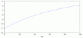
gain= -11.109021/(0.00894395726*Re+1.0)

With this we see the -11.109 that we saw before, but now the gain itself is only -11.109 if Re is made equal to zero (Re='re').
As Re gets larger, the gain starts to get smaller because Re is in the denominator.

We can look at this more too, but for now here are the two schematics and the plot of Gain vs Re where we see some significance creep in with certain values of Re...
Note the gain changes from about -11 to about -6 with change of Re from 0 to 100 Ohms. Typical value is around 10 to 20 ohms i think.
 

Attachments

LvW

Joined Jun 13, 2013
2,035
Hi again,
I dont think it matters if it is a differential quantity or not. It is a quantity, and if that quantity comes about through a DC analysis, then if the DC circuit conditions change then the quantity changes too.
No doubt about this - IF THE DC CONDITIONS CHANGE.

But why do you expect such a change? The dc conditions are given in the task description and remain fixed (all parts values are given).
 

MrAl

Joined Jun 17, 2014
13,765
No doubt about this - IF THE DC CONDITIONS CHANGE.

But why do you expect such a change? The dc conditions are given in the task description and remain fixed (all parts values are given).
Hi,

That is actually the crux of all this.

If you look at Circuit 1 and imagine you calculate the emitter current labeled as "(ie)" with arrow too, then imagine ANY value for 're' that is non zero (like 10 ohms) and place that into Circuit 2, then calculate the emitter current again. You can easily imagine that the DC emitter current changes at least a little anyway.
Now back up a little. We used Circuit 1 to calculate 're' because of the calculated "(ie)" current so what happens if "(ie)" changes once we place the value of 're' (which was previously zero) into the circuit. We get a different 're' and thus a different gain and this is more obvious by the prelim formula i provided.
So we would see:
re1=0.025/ie1
re2=0.025/ie2

and so the gain would be more accurate using re2 rather than re1.

Now how do i know this would really be the case.
It is because the circuits i provided are the DC equivalent of the AC circuits we usually use, and so the AC gain can be calculated from either circuit (mine or Jony's). However, if you use mine then 're' is a resistance that depends on the operating conditions that exist always, not just before we place 're' into the circuit.

Is this starting to make sense now?

Key points:
1. The circuit with the three new voltage sources is equivalent to the AC circuit normally used except it can have 're' in it always.
2. 're' is always the right value no matter what the final DC emitter current is.
3. The difference may be small between using the two different methods, but i would want to handle that on a case by case basis or at least we could look into this by imagining a few circuits with different values than we had been considering here.
4. At the very least you should find this 'new' method very interesting :)
 

Jony130

Joined Feb 17, 2009
5,598
Why no single book I've seen mention that we should use "re" in DC calculation?
I always thought that "re" is pure AC parameter due to its definition
re = dVbe/dIe

Are you assuming piecewise linear model? When we replace the PN junction with a voltage source and a "dynamic" resistance?
 

LvW

Joined Jun 13, 2013
2,035
If you look at Circuit 1 and imagine you calculate the emitter current labeled as "(ie)" with arrow too, then imagine ANY value for 're' that is non zero (like 10 ohms) ..
...........................
Key points:
1. The circuit with the three new voltage sources is equivalent to the AC circuit normally used except it can have 're' in it always.
2. 're' is always the right value no matter what the final DC emitter current is.
3. The difference may be small between using the two different methods, but i would want to handle that on a case by case basis or at least we could look into this by imagining a few circuits with different values than we had been considering here.
4. At the very least you should find this 'new' method very interesting :)
I am sorry - I cannot agree
(or I am completely stupid, because I cannot follow your first cited sentence.)
I only can repeat that for calculating the DC emitter current there is - PER DEFINITION of the DC conditions - no differential resistor (there must not be such a resistance).
 

MrAl

Joined Jun 17, 2014
13,765
Why no single book I've seen mention that we should use "re" in DC calculation?
I always thought that "re" is pure AC parameter due to its definition
re = dVbe/dIe

Are you assuming piecewise linear model? When we replace the PN junction with a voltage source and a "dynamic" resistance?
Hi,

Books are behind the times, some say by one year but i think it varies more or less.
Books often just repeat information that has been given in the past. When there is new research that comes out after the publication date, it's not in the book of course.
Consider this new research but be aware that the differences found could be small due to the bias conditions.

The model i am using is the transistor is replaced with a current controlled current source and includes the 're' resistance. Yes, Vbe=0.65 volts.
See the attachment in that previous post.

I'll try to provide more information soon.
 
Last edited:

MrAl

Joined Jun 17, 2014
13,765
I am sorry - I cannot agree
(or I am completely stupid, because I cannot follow your first cited sentence.)
I only can repeat that for calculating the DC emitter current there is - PER DEFINITION of the DC conditions - no differential resistor (there must not be such a resistance).
1. The circuit with the three new voltage sources is equivalent to the AC circuit normally used except it can have 're' in it always.

Hello,

You can not follow that #1 sentence?
Here's what you can do. Set up the original circuit without 're' in a circuit simulator, complete with the three capacitors and set Vin=0.
Do a static DC analysis. You will find that the three capacitor voltages settle to three static DC voltages, call them E1, E2, E3.
Now you know that for fast signal times E1, E2, and E3 will not change because they are considered to be voltages of capacitors with large values. This allows us to replace the capacitors with those static DC voltage sources.
Now if you did that right, you will have zero volts on the input and zero volts on the very output.
Now increase the input Vin by a very small amount, start with 0.001 volts.
Now observe the output voltage Vout. The gain is then G=Vout/0.001.

That is just to show the equivalence of circuits, but next we would start to look at 're' and it's function in the circuit.
If we calculate 're' with the emitter current from above, we get a certain value, and if we then insert that into the circuit we effectively increase the total resistance at the emitter and thus we change the gain.
If we instead keep 're' in the circuit the whole time, we not only calculate the value from the DC conditions but it remains in there for the AC analysis also.
 

LvW

Joined Jun 13, 2013
2,035
My fault: I forgot to quote the "first senence".
Here is it: "If you look at Circuit 1 and imagine you calculate the emitter current labeled as "(ie)" with arrow too, then imagine ANY value for 're' that is non zero (like 10 ohms)"

That was the sentence I couldn`t follow.
That means I did not speak about the "three new voltage sources" in your text.

Question: Don`t you agree that
* DC equivalent circuit diagrams must contain only quantities which are DC relevant (static quantities) , and
* AC equivalent circuit diagrams must contain only quantities which are AC relevant ?

Further comment: I must admit that I do not understand the contents of your last post:
......"original circuit without re in a circuit simulator...?
The "original circuit" contains a transistor and not any quantities which appear in an equivalent diagram only. And why should I replace capacitors by voltage sources? What is the purpose of the whole described procedure?
 
Last edited:

MrAl

Joined Jun 17, 2014
13,765
My fault: I forgot to quote the "first senence".
Here is it: "If you look at Circuit 1 and imagine you calculate the emitter current labeled as "(ie)" with arrow too, then imagine ANY value for 're' that is non zero (like 10 ohms)"

That was the sentence I couldn`t follow.
That means I did not speak about the "three new voltage sources" in your text.

Question: Don`t you agree that
* DC equivalent circuit diagrams must contain only quantities which are DC relevant (static quantities) , and
* AC equivalent circuit diagrams must contain only quantities which are AC relevant ?

Further comment: I must admit that I do not understand the contents of your last post:
......"original circuit without re in a circuit simulator...?
The "original circuit" contains a transistor and not any quantities which appear in an equivalent diagram only. And why should I replace capacitors by voltage sources? What is the purpose of the whole described procedure?
Hi,

Quote three lines:
Question: Don`t you agree that
* DC equivalent circuit diagrams must contain only quantities which are DC relevant (static quantities) , and
* AC equivalent circuit diagrams must contain only quantities which are AC relevant ?

This is not strictly DC or AC, it is BOTH DC and AC at the same time. There is no need for an AC only circuit now (although we do swap caps with voltages sources). This is a perturbation method which is different than your typical small signal method. It is somewhat similar to a transient analysis but we just look at a tiny input step.
You do realize that you can get small signal results from large signal models right?

Quote two lines:
The "original circuit" contains a transistor and not any quantities which appear in an equivalent diagram only. And why should I replace capacitors by voltage sources? What is the purpose of the whole described procedure?

A spice circuit with a transistor that is made the way we want to analyze this would be made up of a current controlled current source with amplification factor equal to 300 which is the Beta of the modeled transistor. This 'transistor' would also include 're' if we want to include that in the analysis, which we did before so we do that again.
Replacing capacitors by voltage sources is a standard procedure for doing a perturbation analysis. If this is new to you, then you will be learning an entirely new way to analyze circuits for AC. I have to say though i am a little surprised you've never seen this before.
If you like electrical/electronic theory, you will like this i am sure. If you are one of those who just wants shortcuts to circuit analysis, then you may not like this 'new' technique.

You should really try this though as outlined. It's not hard to do although we do have three caps here so you need to use three DC voltage sources once you solve for the three DC cap voltages. As you know, once the caps charge to their nominal voltage level they stay that way on average for an AC analysis. That's the key.
Another way to see this result is to take the transfer function for any quantity and allow the Laplace variable 's' to go to zero. With 's' going to zero we get what is called the 'final' value for each capacitor voltage, and that becomes the DC voltage value.
Another way to see this happen is to do a transient analysis with a very tiny AC voltage as input, but it's harder to get a grip on what is happening there because you have to use an AC source and measure an AC voltage. With the 'new' technique, you are always working with DC quantities although some of them may be very tiny. It's a very interesting way to do it and you can do it with any circuit, even ones that you dont have a small signal model for.

Recap of the method for this circuit...
1. Do a DC analysis with 're' in the circuit already as re=0.025/(ie). 're' depends on the current (ie) which is emitter current.
2. Calculate all the cap voltages.
3. Replace the caps with DC voltage sources that equal the calculated values for each one noting correct polarities.
4. Perturb the input with a small DC voltage like 1mv or maybe even 1uv.
5. Observe the output voltage decrease (or increase).
6. Calculate the gain from Vout/Vin.
Note we didnt even have to calculate 're' because it comes natural as we replaced it with 0.025/(ie) already.
This is simpler to do in a circuit simulator.

The main reason for doing this:
1. When we normally calculate 're' we do that with the static emitter current (ie) from the DC only circuit.
2. When we insert that into the circuit later for the AC analysis, we void the DC analysis in step 1 above because if we really did that the emitter current would change and so the calculated value for 're' would normally change.
3. To get around that without actually using the 'new' technique, we could increase 're' a little by looking at the new current in the DC only circuit, then see if the calculation still works: re=0.025/(ie). We could do this a few times and then we would get a value of 're' that is closer to what we really should have there.

Note the 'old' technique is probably good enough for many things, so the 'new' method is more of an improvement on the old technique. In reality though it's not very 'new' it's just a different way of analyzing an AC circuit and can be used with any AC circuit.
If you like, we can switch to a voltage divider which will show this more clearly most likely.
 
Status
Not open for further replies.
Top