Need help understanding some datasheet details of an IC

Thread Starter

lex4794

Joined Jun 3, 2021
12
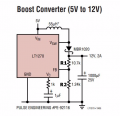
I am trying to build a boost converter to drive a powerful LED. The input will be 21 volts from 5S 18650 batteries to an adjustable 43V-54V (general voltage range) output with a 3A cap. I am looking at an integrated switch DC switching regulator as the center of the circuit. This one in particular because of its 10 amp current capability, its short parts list, as well as the wide input voltage range. Below is the schematic for a 5v-12v boost converter included in the Datasheet (I understand this is for a different chip however, from what I can tell they are functionally the same just with different maximum switch currents and this datasheet has all of the details). Now finally to my question. In the datasheet (page 7), it specifies that the pin (Vc) can be used for current limit adjustment. Specifically, Vc=0.9V is low output current and Vc=2V is high output current. The reference voltage is 1.244 volts at the FB pin with 0.8V at the VC pin. This indicates that I need some sort of potentiometer set up in the circuit to have an adjustable current supply. Would I do so by changing the resistance value of the resistor coming off of the Vc pin, or by changing resistor 2 of the voltage divider going into the FB pin to GND?
I understand that I will have to change some values because I am using a higher voltage.
Please ask if you need me to clarify anything.
boost.JPG
 

Thread Starter

lex4794

Joined Jun 3, 2021
12
Just a note, I have already done the calculations to size the right inductor as well as the right smoothing capacitors for my specific use case.
 

Papabravo

Joined Feb 24, 2006
21,225
1. Can you elaborate on the meaning of: " an adjustable 43V-54V (general voltage range) output with a 3A cap".
2. You are aware that boosting the output voltage by a factor of 2.05 to 2.57 will require larger input currents by those same factors.

The immutable rule of DC-DC conversion schemes is:

Output power will always be less than input power. In some cases it will be much less.
I would not put much faith in using the schematic and BOM for a 5V-12V converter as a template for your project. The power levels are reaching for the nosebleed seats (in excess of 120W). Everything becomes more difficult and more critical and SMPS designs do not scale very well IMHO. I would not count on being successful making this on a breadboard. A well designed PCB will be essential.

I strongly recommend that you try out your ideas on a simulator.
 
Last edited:

Thread Starter

lex4794

Joined Jun 3, 2021
12
1. Can you elaborate on the meaning of: " an adjustable 43V-54V (general voltage range) output with a 3A cap".
2. You are aware that boosting the output voltage by a factor of 2.05 to 2.57 will require larger input currents by those same factors.

The immutable rule of DC-DC conversion schemes is:

Output power will always be less than input power. In some cases it will be much less.
I would not put much faith in using the schematic and BOM for a 5V-12V converter as a template for your project. The power levels are reaching for the nosebleed seats (in excess of 120W). Everything becomes more difficult and more critical and SMPS designs do not scale very well IMHO. I would not count on being successful making this on a breadboard. A well designed PCB will be essential.

I strongly recommend that you try out your ideas on a simulator.
I know that circuits will draw more power as it outputs more power.
I need to have a 3 amp cap (Maximum) with an adjustable power range below that. The LED draws 2.98A at 52.7 volts and around 100mA at 45 volts. The Absolute maximum ratings for the LED are far above this so there is lots of wiggle room, I just can't dissipate that much heat with my current heat sink solution(I have tested this). I will design a PCB for this, however, I will do a low power test on a breadboard just to make sure things work before ordering some PCBs. I am accounting for at least a 20% loss of power due to inefficiencies. boost.JPG
The schematic above is of a much higher voltage circuit (granted not a 160W one). Looking at the component values of this circuit along with the electrical parameters in the datasheet it looked like the values were scalable. I'm guessing that this is a bit risky given the nature of high-power switching circuits?

Why don't you use an LED driver IC? Such as this one:
https://www.diodes.com/assets/Datasheets/AL8853.pdf
At the power levels you are using, an external MOSFET will give a much wider choice of ICs, and the AL8853 will still have a smaller BOM than the device you were looking at.
I was looking at this package before and I don't like how it relies on resistors on the main power stages of the converter going to GND to limit current or voltage. (R6 on the constant current mode and R3 on the constant voltage mode). This would mean that I need a +160 Watt resistor?
 
Last edited:

dl324

Joined Mar 30, 2015
16,935
Would I do so by changing the resistance value of the resistor coming off of the Vc pin, or by changing resistor 2 of the voltage divider going into the FB pin to GND?
Either.
1630431767717.png
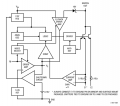
From this block diagram:
1630431913171.png
You can see that the output voltage is:
\(V_{OUT}=1.24V(1+\frac{R1}{R2})=1.24V*(1+\frac{10.7k}{1.24k})=11.94V\)

How long do you expect the circuit to operate using your 5S configuration. If you used 2S2P you could get a longer runtime.
 

Thread Starter

lex4794

Joined Jun 3, 2021
12
I don't know how you get to that figure.
The current sense voltage is 0.2V. Your LED takes 2.93A. That means that the dissipation is 0.6W (0.2V*2.93A)
Oh, oops, perhaps I should have had coffee before posting. That makes sense (no pun intended). So I would need a 0.07-ohm resistor at R6 for the current limit and a 0.27-ohm resistor at R3 for the current sense input meaning there would be at most 2.7 watts of heat dissipated.
boost (2).JPG
 

Papabravo

Joined Feb 24, 2006
21,225
On the LT1270/LT1270A, you cannot just change the resistor values arbitrarily to get the output voltage you want. If R1 >> R2 (Ex R1=34.8K and R2=1.24K) the output will be limited to a bit less than the input because there is so little current flowing in the resistive divider. The FB will not come up to the 1.244 Volts required to get an output higher than the input. According to my simulation it will only rise to 450 mV.

You might want to look up Linear Technology AN-19 (Application Note 19). It details the inner workings of these devices. This is the LT1270 "jig" from the LTspice download with R1 set at 34.8K to output ≈ 44.4 Volts. As you can see it doesn't even come close. the output is one Schottky drop below the input voltage. V(n002) is the voltage on the "FB" pin.

EDIT: You have to run the simulation for a longer time. I was not expecting this behavior


1630433135209.png
 
Last edited:

Thread Starter

lex4794

Joined Jun 3, 2021
12
Either.
View attachment 246945
From this block diagram:
View attachment 246946
You can see that the output voltage is:
\(V_{OUT}=1.24V(1+\frac{R1}{R2})=1.24V*(1+\frac{10.7k}{1.24k})=11.94V\)

How long do you expect the circuit to operate using your 5S configuration. If you used 2S2P you could get a longer runtime.
In order to deal with a more reasonable amount of current, 10A instead of 30A, I opted for a higher input voltage. Have to deal with less heat and yield efficiency gains off of that. Run time at max power(tested with another converter) is about 15 minutes XD.
 

Papabravo

Joined Feb 24, 2006
21,225
Color me humble for not running the simulation long enough. From the standard jig I bumped the inductor to a larger value. This is a boost ratio of just over two times from a 6s 18650 source (3.6V * 6 = 21.6V).

1630434149121.png
 

Thread Starter

lex4794

Joined Jun 3, 2021
12
Color me humble for not running the simulation long enough. From the standard jig I bumped the inductor to a larger value. This is a boost ratio of just over two times from a 6s 18650 source (3.6V * 6 = 21.6V).

View attachment 246948
That is an epic looking simulation, what is the name of the program? Thank you for taking the time to build that! So what your saying is that while I can boost 21 to 54 volts, I may not be able to adjust the output power of the converter on the go, is that the idea?
I've been reading AN-19 and looking at the voltage divider section and I still don't understand how changing the resistor values will not result in a change in the resulting current.

"Design procedure for a boost regulator is straightforward.
R1 and R2 set the regulated output voltage. The feedback
pin voltage is internally trimmed to 1.244V, so output
voltage is equal to 1.244 (R1 + R2)/R2.
....
The 1.24k value for R2 is chosen to set divider current at
1mA, but this value can vary from 300Ω to 10k with
negligible effect on regulator performance. For proper
load regulation, R2 must be returned directly to the ground" AN-19
 

Papabravo

Joined Feb 24, 2006
21,225
That is an epic looking simulation, what is the name of the program? Thank you for taking the time to build that! So what your saying is that while I can boost 21 to 54 volts, I may not be able to adjust the output power of the converter on the go, is that the idea?
I've been reading AN-19 and looking at the voltage divider section and I still don't understand how changing the resistor values will not result in a change in the resulting current.

"Design procedure for a boost regulator is straightforward.
R1 and R2 set the regulated output voltage. The feedback
pin voltage is internally trimmed to 1.244V, so output
voltage is equal to 1.244 (R1 + R2)/R2.
....
The 1.24k value for R2 is chosen to set divider current at
1mA, but this value can vary from 300Ω to 10k with
negligible effect on regulator performance. For proper
load regulation, R2 must be returned directly to the ground" AN-19
I apologize for jumping to a premature conclusion based on running the simulation for a limited time. I posted both to illustrate where (and maybe how) I went wrong. To make this design adjustable, you could replace R1 with two resistors and a pot between them. You want to ensure that whatever setting the pot has, the output will be within a certain range. The two resistors will set the minimum output and the two resistors plus the pot will set the maximum output.

The simulation program is called LTspice, and it is a free download from ADI (Analog Devices Inc.). They acquired Linear Technology a coupe of year ago and inherited the simulator in the process. They continue to support it and update their model libraries.

LTspice Simulator | Analog Devices

There are additional online resources for learning how to use it and adding additional models of interest to your own personal collection. We have an active community of LTspice users here so you can always ask questions and be assured of prompt and useful answers. There is an LTspice user's group on groups.io but they focus on issues with the operation of LTspice and not on the actual designs and simulations that people run. IMHO their site is of limited utility and they can be snarky.
 
Last edited:
Top