
Hi AAC,
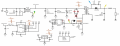
I am building a flyback DC/DC converter whose driver circuit is being fed from the same supply as the converter itself. I am not using the AUX winding option. See attached schematic and oscilloscope results. The scaling factors are correct.
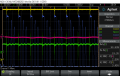
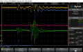
Background: When I turn off on the flyback switch, there are switching transients at VDS and the supply due to parasitic leakage current being circulated around the circuit – since that parasitic resonant current has to go somewhere, obviously. This is a fact of DC/DC circuits I cannot change too much. But what is especially causing me a headache is the fact that these same turn-off transients are reverberating all over my control circuit as well. This causes problems in the gate drive. I’m running into problems of accidental FET turn on, FET avalanching, and transformer and FET overheating issues. I have attached a schematic and test results in this circuit to show for example how transients can reach my +5V LDO supply – which is the source of controller problems downstream. The green probe in my circuit is a differential probe and unfortunately I only have one. The brown overhead pictures show some places where these switching transients are popping up. My transformer operates heavily in DCM as you can tell. If I can make it operate closer to critical conduction mode I think that would be good. Although I'm also trying to figure out how to do that effectively since my load is very highly variable.
Question: What schematic, and/or PCB layout tricks can I do to prevent, or at least drastically mitigate even more, the impact these transients can have on the driver circuit feeding the FET gate? I’ve flooded the switching node and common planes as much as I could on the PCB, tried separating high current grounds from analog/digital grounds, and added some filtering to the DC/DC brick. What can you recommend for other protection/transient suppression schemes in order to protect my controller and MOSFET? Further, remember that these are repeated transients at 165kHz (+/- 75kHz) so the protection would have to operate (almost) continuously. You can ignore the magenta waveforms in my test results. Any suggestions and brainstorming is very welcome.
I am building a flyback DC/DC converter whose driver circuit is being fed from the same supply as the converter itself. I am not using the AUX winding option. See attached schematic and oscilloscope results. The scaling factors are correct.
Background: When I turn off on the flyback switch, there are switching transients at VDS and the supply due to parasitic leakage current being circulated around the circuit – since that parasitic resonant current has to go somewhere, obviously. This is a fact of DC/DC circuits I cannot change too much. But what is especially causing me a headache is the fact that these same turn-off transients are reverberating all over my control circuit as well. This causes problems in the gate drive. I’m running into problems of accidental FET turn on, FET avalanching, and transformer and FET overheating issues. I have attached a schematic and test results in this circuit to show for example how transients can reach my +5V LDO supply – which is the source of controller problems downstream. The green probe in my circuit is a differential probe and unfortunately I only have one. The brown overhead pictures show some places where these switching transients are popping up. My transformer operates heavily in DCM as you can tell. If I can make it operate closer to critical conduction mode I think that would be good. Although I'm also trying to figure out how to do that effectively since my load is very highly variable.
Question: What schematic, and/or PCB layout tricks can I do to prevent, or at least drastically mitigate even more, the impact these transients can have on the driver circuit feeding the FET gate? I’ve flooded the switching node and common planes as much as I could on the PCB, tried separating high current grounds from analog/digital grounds, and added some filtering to the DC/DC brick. What can you recommend for other protection/transient suppression schemes in order to protect my controller and MOSFET? Further, remember that these are repeated transients at 165kHz (+/- 75kHz) so the protection would have to operate (almost) continuously. You can ignore the magenta waveforms in my test results. Any suggestions and brainstorming is very welcome.
Attachments
-
 158.4 KB Views: 11
 -
 65.9 KB Views: 11
 -
 34.5 KB Views: 11
 -
 40.2 KB Views: 11


