NCP167 explain

Thread Starter

STech2106

Joined Jul 8, 2023
43
Hi guys.
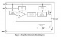
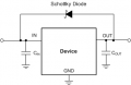
I stumbled across this in the onsemi NCP167 LDO regulator, which I must say looks really powerful onthe spec sheet. In my project, I have a Power MUX that supplies the LDO input at 5V with a total capacity of about 47uF or slightly higher. At the output, I would like to put capacitors of various capacities to filter different frequencies, with a total capacity of 100uF. In the “Enable Operation” section of the datasheet, onsemi describes the functionality of the EN pin and, as you can see internally, there is a MOSFET used for active discharge. I wonder if, when the system is turned off, this is effective in discharging the output capacitance so as not to expose the LDO to a negative voltage generated by the reverse current, or if it would be better to introduce a classic diode with the cathode connected to the input voltage and the anode connected to the regulator output?

How complicated would it be to replace this package if it failed?
 

spenkmo

Joined Apr 24, 2025
25
The internal MOSFET controlled by ~EN is not for active discharge. When EN is low, the MOSFET is on, basically creating an short-circuit at the output of the LDO; this further triggers the "enable" logic that disables the output. This is also why Onsemi claims that the device can endure unlimited output shortage; the protection mechanism is basically the same as setting EN to low. At power off, the MOSFET may or may not have a short period being on, depending on many factors. But it shouldn't be used as a means to providing a discharge path.
 

Thread Starter

STech2106

Joined Jul 8, 2023
43
@spenkmo
The internal MOSFET controlled by ~EN is not for active discharge. When EN is low, the MOSFET is on, basically creating an short-circuit at the output of the LDO; this further triggers the "enable" logic that disables the output. This is also why Onsemi claims that the device can endure unlimited output shortage; the protection mechanism is basically the same as setting EN to low. At power off, the MOSFET may or may not have a short period being on, depending on many factors. But it shouldn't be used as a means to providing a discharge path.
Very strange. Attached is the block diagram of the LDO, which mentions “Active Discharge.”
 

Attachments

panic mode

Joined Oct 10, 2011
4,864
that is possible although not ideal. all of the NCP167 regulators are low output voltage and adding diode will cause significant voltage drop. if you use schottky diode that drop will be smaller but likely still hard to ignore....
 

Thread Starter

STech2106

Joined Jul 8, 2023
43
that is possible although not ideal. all of the NCP167 regulators are low output voltage and adding diode will cause significant voltage drop. if you use schottky diode that drop will be smaller but likely still hard to ignore....
The diode would not be in series but like the attached picture, I don't think this would cause a voltage drop on the output
 

Attachments

panic mode

Joined Oct 10, 2011
4,864
you are right. that would not cause voltage drop when regulator is powered - it would allow output circuit to discharge when input side is voltage is lower, meaning if there is a continuity path (bleed resistor or whatever).
 

Regected424

Joined Nov 27, 2022
8
Why not just put a pulldown resistor on the enable pin? When power is off, enable goes low and goes into discharge mode (assuming you are using the "a" variant). It's also a good idea to have an RC filter on the enable by default if there is any chance of noise. This gives you a clear operational state of the LDO at all times. I do this with more mission critical applications, but it never hurts to be over prepared than trying to debug an unknown state fault.
 

Thread Starter

STech2106

Joined Jul 8, 2023
43
Why not just put a pulldown resistor on the enable pin? When power is off, enable goes low and goes into discharge mode (assuming you are using the "a" variant). It's also a good idea to have an RC filter on the enable by default if there is any chance of noise. This gives you a clear operational state of the LDO at all times. I do this with more mission critical applications, but it never hurts to be over prepared than trying to debug an unknown state fault.
Hi @Regected424 ,
As suggested, it would appear that the enable pin is not intended for discharging the capacitor. However, I searched the ON Semiconductor website for version “a” of the NCP167. There do not appear to be any versions other than “a.” Have you tested this LDO directly in the field? Would it be correct to create a voltage divider to keep EN greater than 1.2V when VIN is present and then send it low?
 

Regected424

Joined Nov 27, 2022
8
I'm just pulling data from their datasheet. The block diagram has a notation at the EN driving an inverted signal to a MOSFET. This MOSFET ties the output to ground. So, the EN is technically not draining, but it is controlling the draining. As far as the "A" version, it is the extended part number. Look to the bottom of the datasheet (page 10), and you will see the options of voltages and packages. In the description, it says if it has active discharge or not.

Matter of fact, the Enable Operation describes in great detail how this works. If nothing is on the EN pin, it is pulled low through an internal 200nA current source. When EN is below 0.4V, the output is discharged to GND through a 280ohm resistor. If you were to add a voltage divider between Vin and GND to feed EN 1.4V, that would give you a pulldown on EN when Vin drops, thus connecting the discharge circuit to the output.
 
Top