Smells like piezo to me; that's a good thing. I say to go forward assuming it is a piezo. If two gates in parallel can't drive it, we can adapt the circuit. Where are you located?
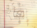
I put this drawing together so you can see how I interpret how to connect this.
Q: which direction do the caps go. I have ordered bi-directional caps but if I wanted to test it with what I have now.
Q: the negative going to the peizo. What type of trigger is that? Rising/ falling edge?
Q: Did I place the ic conditioner cap in the correct place? From the ic's + to cap to ground.
Most of all a huge thank you. I appreciate all from the group and its members.
Capacitors are either polarized (like most electrolytics), or non-polarized (like most ceramics and films). Unless explicitly stated or noted by the schematic symbol, a cap is assumed to be non-polarized and you can connect it either way.
The gate pulls the - end of the piezo down to GND to activate the device. When the piezo is off, the gate(s) output is high, very close to Vcc, and there is nto enough voltage across the device to activate it.
The gate pulls the - end of the piezo down to GND to activate the device. When the piezo is off, the gate(s) output is high, very close to Vcc, and there is nto enough voltage across the device to activate it.
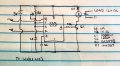
You show all inputs of the logic gates connected together.
The circuit's input voltage is not shown.
The part number and voltage of the voltage regulator are not shown. It needs an output bypass capacitor.
You show all inputs of the logic gates connected together.
The circuit's input voltage is not shown.
The part number and voltage of the voltage regulator are not shown. It needs an output bypass capacitor.
I did think that was odd being all connected together but that's how
It supposed to be. I had a cap in the wrong place. Perhaps that's why it looks strange to a pro. I posted an update with the correction. I added the chips part number and some uppercase "S's" for you. I used a number 2 spongebob pencil and did my best to replicate the font style of Arial Bold. I do not know what an output bypass cap is or where to place it. The voltage is 5.5dc.
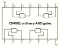
Now you show a CD4081 instead of a CD4093. Why not copy the correct image from Google?
The voltage regulator is missing a part number, voltage and output capacitor.
I'm unsure if the Audio fella is helping or confusing me. I'm having difficulty trusting his posts. I put my software skills to work and I have blocked him.
The drawing is for a discussion in this conversation. My post is to determine if I have wired your schematic correctly. I do thank you.
I assume the sketch is correct now and I have placed the conditioner (cap2) in the right place.
Audioguru is one of the most intelligent resources on here. You may have made a mistake blocking him, IMHO.
If you find his posts confusing, I suspect it’s because of a lack of understanding. Rather than blocking him, you’d be better off trying to understand what he has said.
Audioguru is one of the most intelligent resources on here. You may have made a mistake blocking him, IMHO.
If you find his posts confusing, I suspect it’s because of a lack of understanding. Rather than blocking him, you’d be better off trying to understand what he has said.
Telling me I'm lazy? my drawing is a scribble? I understood it perfectly. Very intelligent.
There are many entries on this post. Having to scroll past insults is basically out of scope of this thread. Filtering him out was so I could focus on what the others were offering.
My apologies to you, the group, and Audioguro.
Cheers
Somebody else said you are lazy. Instead I said that your lack of straight lines and missing details is a scribble.
Why not copy accurate images from Google and paste into Microsoft Paint program?
Who is blocked? You?
Somebody else said you are lazy. Instead I said that your lack of straight lines and missing details is a scribble.
Why not copy accurate images from Google and paste into Microsoft Paint program?
Who is blocked? You?
Sometimes we forget to turn off the 12v led lights so I'd like to activate the relay through this 555 and apply a delayed off of about 10-15 minutes so the relay is automatically disengaged if we forget to turn off the light.
I altered this circuit so it connects to the circuit we have created in this thread.
Pin 2 of the 555 is triggered from the 4093 NAND gate. I would connect pin 2 to the output of the gate that connects to the speaker. I would connect pin 4 to the output from the touch pad. I understand output connected to the speakers (-) lead is held high until the touch sensor is pressed. It then drops to 0v causing the speaker to sound for 750ms which is controlled by C1 & R1. And the constant 5v from the touch pad will satisfy the 555 so it functions. Im hoping that is what is necessary to start the 555.
When the touch pad is pressed a second time the 5v from the touch pad is brought to 0v causing the 555 to reset. From what I understand pin 4 must have current to function so the 750ms pulse coming from the gate to pin 2 would be ignored.
So would this work correctly? If not can you help me configure this properly?
Thank you in advance.
 Facebook
 Google
 GitHub
 Linkedin