NAND gate outputs voltage

Thread Starter

ThomCircuit

Joined Feb 4, 2020
45
And yet they are not on the schematic, so we don't know how they are being treated to prevent overheating, oscillation, and other problems that will affect the one gate you are using. CMOS parts are finicky, and that near-infinite input impedance has consequences.

Note - adding pin names, or at least numbers, to the parts will help us understand what you are trying to do.

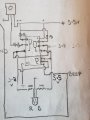
Here is my first guess at your schematic, re-drawn for clarity. I added treatments for the unused gates.

I suppose this circuit can work, but I'm not sure how. Your schematic shows an unknown resistor in series with the 555 power pin (shown here as RX1), and the discharge output (pin 7) applying a dead short to ground on the touch module output. My library has the CMOS 555 in it, but your schematic indicates the original bipolar version, another source of operating issues. In general, it is very bad practice to power an IC from a signal output of another device rather than from a true power supply connection. However, my guess is that relatively high impedance source is what is giving you a time delay. What is the purpose of R2?

Note - many schematic programs hide common device power and GND pins to improve overall clarity and readability. This is why neither IC has explicit power pins in this schematic. If the resistor in series with the 555 Vcc pin were retained, I would have to make a new 555 decal with a power pin that is not invisibly connected to the net named Vcc.

ak
View attachment 203826
I totally agree with you on powering the 555 from the gate. I'm just trying to get this right. In my software programming days I also would not trigger one module with a result of another. It's too difficult to follow. But I have not been able to figure out how to take the result from the gate and trigger the 555 the correct way. With a pulse to pin 2. I just cannot figure out how to do it. Can you help me with this? I also re did my schematic some. All resistors on the 555 are 10k. I remapped the gate logic so the results had the same 3.5volts and then sent the outputs from that into a third so the result is on one signal. (The 555 will beep each time). I'll upload it in a single post.
 

Thread Starter

ThomCircuit

Joined Feb 4, 2020
45
Are you married to the idea of using a 555? If not, everything can be done with one hex inverter (CD40106) and three small transistors.

Also, what is the power source for the circuit?

Please post links to the devices in post #15.

ak
I am happily married. And I need to use this 555 for budget reasons
 

BobTPH

Joined Jun 5, 2013
11,524
You can parallel the gates to get a higher drive capability. This will raise the output voltage if the load stays the same,

Bob
 

AnalogKid

Joined Aug 1, 2013
12,143
Here is a re-work of your circuit. It uses the touch module output only as a signal, not as a power source. Because you want the beep on the rising edge, driving a 555 trigger input will not work. In this circuit, the 555 is acting as a simple inverting power buffer with a hysteretic input.

ak
Closet-Light-2-c.gif
 

AnalogKid

Joined Aug 1, 2013
12,143
Here is a version that eliminates the 555, and replaces it with two of the unused gates you already have. I show an external transistor driving the beeper because I don't know the beeper current requirement. If it is low enough, the 4th gate can be added in to drive it directly. The transistor does not have to be a FET. If you nave a small NPN (2N2222, 3906, 4401, etc.), it will work with an added base resistor.

ak
Closet-Light-3-c.gif
 

AnalogKid

Joined Aug 1, 2013
12,143
That last post triggered a thought. This is about as minimal as I can go with the parts you already have. Now I'm happy.

R1 and C1 set the beep time, approx. equal to 1.1 x R x C. I use a 2.2 uF ceramic because I have a bunch of them.

C2 is the power decoupling cap. It can be whatever C1 is, and should be as close as possible to the 4011's power and GND pins, with short leads.

R2 adds hysteresis to the switching circuit so there is not a noise burst on the output caused by the slow fall time at the inputs.

ak

Closet-Light-4-c.gif
 
Last edited:

Thread Starter

ThomCircuit

Joined Feb 4, 2020
45
You can parallel the gates to get a higher drive capability. This will raise the output voltage if the load stays the same,

Bob
If I understand you right I did this earlier here is the result. The output is the full 5.5 volts. My issue is still taking that output and triggering the 555 with it. I'm just getting a bit lost here.
 

Attachments

Thread Starter

ThomCircuit

Joined Feb 4, 2020
45

AnalogKid

Joined Aug 1, 2013
12,143
A wiring diagram and a schematic are not the same thing. They have different information for different purposes. If you draw out the four gates as individual schematic elements, it will be much easier for us to evaluate your circuit.

Beeper data - voltage range, current, link to vendor page, photo - ?

ak
 
Last edited:

Thread Starter

ThomCircuit

Joined Feb 4, 2020
45
A wiring diagram and a schematic are not the same thing. They have different information for different purposes. If you draw out the four gates as individual schematic elements, it will be much easier for us to evaluate your circuit.

ak
I'll be doing that in the future
 

AnalogKid

Joined Aug 1, 2013
12,143
What is this for?
Power supply decoupling. Circuits expect a power source with a very low impedance at all frequencies. The cap acts as a lowpass filter to keep noise on the power wiring from causing false state changes. It also filters noise generated by the chip from getting out on the power wiring and into other circuits. It also acts as a small battery to provide extra charge when the output changes state and briefly draws more current. The rules of thumb are one cap per chip power pin, located as close as possible to it, with the shortest possible leads.

ak
 

Audioguru again

Joined Oct 21, 2019
6,826
The schematics by Analog Kid show no power supply voltage. With a supply that is only 5V the CD4011 gate has an output current of only a few mA so the 1k current-limiting resistors are reducing the current into the LEDs when the resistors are not wanted and are not needed.
With no current-limiting resistors and a 5V supply the LED current is only 3.5mA. Using 3 gates in parallel then the LED current without any current-limiting resistors will be only 10.5mA but much brighter. Two transistors can be added to make the LED currents higher which would make them brighter.

I don't know how much current the beeper uses so adding a transistor will help make it louder.
 

Thread Starter

ThomCircuit

Joined Feb 4, 2020
45
What do you mean by "gate4"?

ak
The NAnd gate has 4 outputs. I was referencing one of them as gate4. Specifically the one that sounds the buzzer.

Thank you for the explanation of the Power supply decoupling. While I can create it I do not know how to add it in the circuit.
 

Thread Starter

ThomCircuit

Joined Feb 4, 2020
45
Power supply decoupling. Circuits expect a power source with a very low impedance at all frequencies. The cap acts as a lowpass filter to keep noise on the power wiring from causing false state changes. It also filters noise generated by the chip from getting out on the power wiring and into other circuits. It also acts as a small battery to provide extra charge when the output changes state and briefly draws more current. The rules of thumb are one cap per chip power pin, located as close as possible to it, with the shortest possible leads.

ak
Ok. I googled it. I did not think I'd find it so quick but I get it. I see where it goes. It is connected to the +/- of the ic chip
 

Attachments

Top