 Facebook
 Google
 GitHub
 Linkedin
Hi there
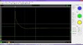
I am looking for some assistance in understanding the Vds waveform I measure when switching off an N-ch enhancement mode power mosfet. The transistor is simply switching off a filament lamp that draws about 5A from the 12Vdc supply. The waveform attached has Vgs on channel 1 and Vds on channel 2.
I am thinking that the spike and discharge curve is due to some parasitic components of the transistor. The transistor is being driven very quickly with a 4A driver with no gate resistor.
Has anyone ever seen a similar voltage at the output that can shed some light on the cause?
Any help is much appreciated.
Thanks
Attachments
-
 334.6 KB Views: 48
")


