MOSFET tester

Thread Starter

Wendy

Joined Mar 24, 2008
23,415
Here is my latest brain part on LL MOSFET. Partly it is to help me verify my understanding is correct, the other is to audition the components I have for their usefulness.
555 voltage booster
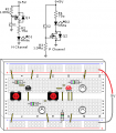
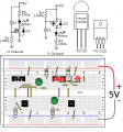
so here are the schematics and the layout. If anyone sees a problem with what I am doing please let me know before I let the magic smoke out. I have replaced the old image with the working version. I kept the old image below as a reference for anybody who might not have seen the old one. The brain farts were flowing wild and free in in the making of this, if you remove the LED you can measure the conductance between the drain and source as long as you pay attention to the polarity. All it is not clear on the drawing a bracket where the MOSFETs go to prevent problems further down the line. If using higher voltages change R2 and R4 for larger values suitable to drive the LEDs.

MOSFET tester #4.png

Oops I thought I had finished it, I will fix it tomorrow.

I got it working finally, I also printed a box for the protoboard since I am not going to tear this down, but keep it for future use. I went ahead and attached the STL files to print the enclosure I have made for this.

220808 Shrunk.jpg

20220808_165807.jpg

I left two holes in the bottom of the package to put 5/8" by 1/16" niobium magnets to use with my steel workbench.
 

Attachments

Last edited:

dl324

Joined Mar 30, 2015
16,846
It's more conventional to use N channel to switch low side and P channel to switch high side.

As drawn, the body diode in the P channel MOSFET will always be conducting; S2 is ineffective. The source should be at a more positive voltage than the drain.

S1 will turn off Q1. Is that what you intended?

EDIT: Note that the original post has been modified, so these comments may no longer be relevant.
 
Last edited:

Thread Starter

Wendy

Joined Mar 24, 2008
23,415
Thank you. That is the kind of feedback I was hoping for. I will try to fix it tomorrow.
 

Ian0

Joined Aug 7, 2020
9,677
It seems to me that the circuit labelled "P-channel" would be perfect for testing N-channel devices, and the circuit labelled "N-channel" perfect for testing P-channel devices. (and something has gone a bit awry with your symbols)
 

Alec_t

Joined Sep 17, 2013
14,280
With a 5V supply and the white LED having a Vfwd of 3V, that only leaves 2V for the N-FET gate switching voltage. A similar problem arises with the P-FET tester.
The N-FET would be better for low-side switching, and the P-FET for high-side switching, as dl324 says.
 

Thread Starter

Wendy

Joined Mar 24, 2008
23,415
OK latest brain fart (hopefully last revision):

LL MOSFET tester.png

part of the reason I am doing this project is to finally try to understand how to bias MOSFETs.
 
Last edited:

Thread Starter

Wendy

Joined Mar 24, 2008
23,415
As far as I know the diode and the direction of the arrow determine which polarity goes where. Would it be a correct statement to say that most moffetts have the diode across the drain source?
 

crutschow

Joined Mar 14, 2008
34,285
Would it be a correct statement to say that most moffetts have the diode across the drain source?
That connection actually determines which is the source terminal.
MOSFETs are bi-directional so, if you have access to the substrate connection, you can connect that arbitrarily to either terminal, which will dictate that terminal as the source.
 

Thread Starter

Wendy

Joined Mar 24, 2008
23,415
I have finished this project. And put the revised final drawing in the first post. I even printed an enclosure for this board since I am not going to tear it down. While it qualifies for the completed projects forum I am going to put it in my protoboards projects instead.
 

Thread Starter

Wendy

Joined Mar 24, 2008
23,415
So this is my final iteration:

MOSFET tester #4.png
I replaced the resistances on the LED's to allow for 12 votes. As it happens I pulled the wrong data sheet for my other N channel MOSFET. So I am attaching the updated data sheets here as well as putting them in the data sheet archive. The next step is to put a ohm meter across the source and drain, and see what voltage they switched by the simple expedient by of changing the power supply voltage. I will post the results of this experiment presently.

I had a bit of a problem with one of the wires making intermittent contact to ground on coordinate A 9, during one of my buying sprees I had bought 22 gauge jumpers (not preferred because I have trouble getting some wires into a protoboard, I typically use 24 gauge).
 

Attachments

Last edited:

dl324

Joined Mar 30, 2015
16,846
The next step is to put a ohm meter across the source and drain, and see what voltage they switched by the simple expedient by of changing the power supply voltage.
Measuring resistances in a powered circuit is not advised. You have to calculate the S/D resistance. Resistances are typically specified for certain conditions. This is what AO3400 use:
1660855535023.png
1660855552620.png
1660855580965.png
1660855484699.png
 

Thread Starter

Wendy

Joined Mar 24, 2008
23,415
I will disconnect any power connections to the source and connect to it directly. It should work fine. And of course, I will play pay attention to the polarity of the leads.
 

Thread Starter

Wendy

Joined Mar 24, 2008
23,415
Whew, I finally got the S.O.B. right. Somewhere with all the revisions I messed up the pins on the TO220 case. Wasted a huge amount of time looking for it. Interesting part, normal MOSFETs still switch at 5 volts. Although probably not all the way now to get the measurements.

MOSFET tester #4.png
 
Last edited:

Thread Starter

Wendy

Joined Mar 24, 2008
23,415
And here are the results:
Meter shorted 0.3Ω
IRF9540 P channel
5V 0.6Ω
12V 0.6Ω
VP2206 Logic Level P channel
5V 1.3Ω
16N05L Logic Level N channel
5V 0.8Ω
IRF520 N channel
5V 1.1Ω
12V 0.9Ω
TN1060 Logic Level N channel
5V 3.1Ω
 
Top