 Facebook
 Google
 GitHub
 Linkedin
Hello everyone,
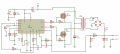
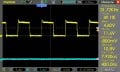
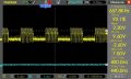
I am trying to make DC - DC converter using SG3525. (fig. circuit diagram). in circuit diagram i make some changes. i remove full bridge rectifier, change mosfet to IRF3205 and remove feedback circuit which is connected to inverting input (pin 1). i connect a 220 volt bulb (load) to secondry side of ferrite core trasnformer to check every things work fine or not. I check the gate waveform and drain source waveform which show in attachment figure pic_gate waveform and figure pic_drain waveform. when i connect load ( 220v bulb) on secondry side of transformer waveform gate waveform are distorted which can see in figure gate waveform.
I dont have any idea what happen. please tell me how can i resolve them.
Attachments
-
 299.1 KB Views: 24
 -
 133.3 KB Views: 22
 -
 132 KB Views: 23
 -
 147.5 KB Views: 23


