MOSFET help

Thread Starter

Peter Olt

Joined Dec 15, 2015
19
I'm new to this group, so firstly, a big hello and thank you for allowing me to join this cool community!

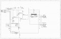
I am a new product designer and have a MOSFET issue I would love some help with if possible. We had a small automotive product that uses an IPD90P03P4L to turn on a 12 VDC compressor that draws about 25 amps. So far, so good and there are about 3000 of these units working happily all around the country.

But, now we want to run the Compressor at 80% PWM for 0.15 seconds before it goes to 100% PWM. It works fine, but if I run it at 80% PWM for more than a few seconds the MOSFET gets quite warm. The PWM is at 1000 hertz by the way.

I would love to get some advice on how to better protect the MOSFET from whatever spikes seem to be occurring.

We do have a TVS across the Compressor (SA36A TVS DIODE 36VWM 58.1VC DO204AC) that we have found to be vital, without this the MOSFET will fail in few dozen operations.

We have to resolve this over the next few days and would be happy to pay for some expert help with this.

Please let me know if anyone is interested / available.

Best Regards,

Peter
 

bertus

Joined Apr 5, 2008
22,278
Hello,

Do you have a schematic of your setup?
It sound like the switching times are to long.
During the transitions the MOSFET is in the linear reagion and will get warm.
There might be some enhancements for the driver needed.

Bertus
 

dl324

Joined Mar 30, 2015
16,935
Your inaugural post; welcome to AAC!

Schematics or other diagrams are always appreciated; well drawn ones even more so.

What do you mean by PWM at 80% and what does 100% mean?

The motor in your compressor is an inductive load. A TVS might help, but it's more typical to use a diode to protect the switch.
 

cmartinez

Joined Jan 17, 2007
8,257
Driving a Mosfet properly is serious business. As has already been requested, a schematic would come in handy for us to try to help you out.
 

Thread Starter

Peter Olt

Joined Dec 15, 2015
19
Hi guys, okay I attached a full schematic. Some clarifications;

  • By "PWM" I mean "Pulse Width Modulation".
  • PWM refers to how the MOSFET Q1 is being driven for 0.15 seconds at an 80% On and 20% OFF duty cycle. This is what is causing Q1 to heat up, but only if I run it on the 80/20 PWM for an extended period, say over 5 seconds. In normal operation it will only run in the 80/20 mode for 0.15 seconds, and then it will go to 100% (fully ON) mode, whereby Q1 doesn't even get faintly warm, no matter how long it is running.
Some Questions:
  1. I would like firstly establish if we have the circuit designed correctly, especially considering the change to now running Q1 on a PWM cycle instead of formerly just ON or OFF.
  2. Secondly, we have a reverse polarity diode (D5) fitted but I am concerned this may be much slower reacting then the TVS's (D7 and D6) and so may render the TVS's ineffective? Should we dispense with D5?
  3. Thirdly, I would like to explore the best choice for spike protection - current TVS? another type of TVS? Or a Schottky Diode?
  4. Is the heating up of Q1 "normal" and if so, should I even be worried about it, considering that it normally only runs in the PWM mode for 0.15 seconds?
Thanks in advance for any help you may be able to offer,

Kind Regards,

Peter
 

Attachments

MaxHeadRoom

Joined Jul 18, 2013
28,696
Any reason you are using a P channel instead of designing for a N channel?
It is rated at 90amps so I it could be the fact it is not turned fully on causing the heating?
I would have tended to use a mosfet for Q3 such as 2n7000.
Max.
 

cmartinez

Joined Jan 17, 2007
8,257
Any reason you are using a P channel instead of designing for a N channel?
It is rated at 90amps so I it could be the fact it is not turned fully on causing the heating?
I would have tended to use a mosfet for Q3 such as 2n7000.
Max.
I agree, a 2n7000 would've been a far better choice, but if he wants to stick to the 3904, then I'd suggest changing R2 and R3 to 470 ohms. Maybe 10K is not allowing enough current to flow through the transistors, at first glance.
Also, R4 and R5 have too high a value too, IMHO.
 

bertus

Joined Apr 5, 2008
22,278
Hello,

What is D5 doing at the negative terminal?
How does the ground reach the controller?
I assume D7 is the TVS diode.

Bertus
 

Thread Starter

Peter Olt

Joined Dec 15, 2015
19
Any reason you are using a P channel instead of designing for a N channel?
It is rated at 90amps so I it could be the fact it is not turned fully on causing the heating?
I would have tended to use a mosfet for Q3 such as 2n7000.
Max.
Hi Max,
I think a P Channel was originally chosen because the circuit need to have a (+) output. The new application would now allow either the (+) or (-) to be switched by the MOSFET, it an N Channel better?

Thats a very good point about using a MOSFET for Q3, I assume this would provide a cleaner more definite signal to Q1?
 

Thread Starter

Peter Olt

Joined Dec 15, 2015
19
I agree, a 2n7000 would've been a far better choice, but if he wants to stick to the 3904, then I'd suggest changing R2 and R3 to 470 ohms. Maybe 10K is not allowing enough current to flow through the transistors, at first glance.
Also, R4 and R5 have too high a value too, IMHO.
Thank you, that's another very good suggestion, I could make a test circuit and prove this out. I guess I will need to decide if changing Q3 and Q4 to mosfets might be good to do and how this will affect the value of the resistors you are referring to.

Would you (or someone else) be willing to redesign this circuit as a paid project? The issue I have is that we need to finalize this design in the next few days and get the board design finalized and to a board house.

Thanks, Peter
 

cmartinez

Joined Jan 17, 2007
8,257
It looks like it's the current limit resistor for D4 which must be a 5V zener; I can't tell, the text is too small.

EDIT: Bertus beat me by seconds...
*slap in the forehead* .... a zener!, at first I couldn't tell either for the same reason as you...
 

crutschow

Joined Mar 14, 2008
34,459
It looks like your spike and reverse-bias protection is okay.

The heating is likely due to the large 10kΩ pull-up resistor at the gate of the MOSFET which is causing the transistor to turn off slowly due to the IPD90P03P4L-04 MOSFET gate charge of 125nC typical.
My simulation of this circuit causes a transistor turn-off time of about 0.1ms and a dissipation of about 7W for a 1KHZ PWM.
Changing the resistor to 1kΩ reduced the fall-time to about 10μs and the dissipation to about 2W.

That being said, there's likely no problem in operating the device as you have it as long as you don't run in the PWM mode for more than a few seconds.
 

Thread Starter

Peter Olt

Joined Dec 15, 2015
19
Hello,

R1 seems to be the current limiting resistor for the zener to power the controller.

Bertus
Hi Bertus,
Yes, you are right about R1 and D4 is a 5 volt zener to run the micro.
What is D5 doing at the negative terminal? - It was originally to proof the circuit against reverse polarity if installed incorrectly. However the tests I did with an amp meter in series with the TVS showed that when D5 was in circuit the TVS current dropped to 0.00. When D5 was shorted the TVS drew 0.8 amps, so I assumed from that it was doing its job protecting Q1 from spikes. I concluded that we D5 probably is a liability and should be removed, any thoughts?
How does the ground reach the controller? - Through pin 2 on connector J1 then to the vehicle chassis.
I assume D7 is the TVS diode. - Yes, correct, part # SA36A by Vishay.
 

Thread Starter

Peter Olt

Joined Dec 15, 2015
19
It looks like your spike and reverse-bias protection is okay.

The heating is likely due to the large 10kΩ pull-up resistor at the gate of the MOSFET which is causing the transistor to turn off slowly due to the IPD90P03P4L-04 MOSFET gate charge of 125nC typical.
My simulation of this circuit causes a transistor turn-off time of about 0.1ms and a dissipation of about 7W for a 1KHZ PWM.
Changing the resistor to 1kΩ reduced the fall-time to about 10μs and the dissipation to about 2W.

That being said, there's likely no problem in operating the device as you have it as long as you don't run in the PWM mode for more than a few seconds.
Hi Crutschow,

Thank you, this makes a lot of sense. So, if I drop the pull-up (R4 and R5) to 1 k each, do I also change the value of R2 and R3? Do you feel a transistor will work fine, as opposed to changing Q3 and Q4 to mosfets as another very helpful member suggested?
 
Top