MOSFET Gate charging current

Thread Starter

Xavier Pacheco Paulino

Joined Oct 21, 2015
728
Hi,

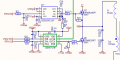
As it is known, the MOSFET is a voltage controlled device. But an instantaneus current is needed to charge the gate capacitance according to

Ic = C(dv/dt)

I have a gate driver which specifies a peak current of 5A. So for design purposes, do I choose any current below this rating, right? Do I need to extract from the datasheet the total gate capacitance to calculate this? I think that I have to add a gate resistor to limit the current to the value that I select, right?
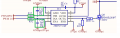
 

Thread Starter

Xavier Pacheco Paulino

Joined Oct 21, 2015
728
It isn't typical to try to limit gate charging current. Doing that slows MOSFET switching time.
The gate will take whatever the driver will provide.
For example, according to this app note: https://www.infineon.com/dgdl/Infin...N.pdf?fileId=5546d462518ffd8501523ee694b74f18

"The current, charging and discharging the gate, is limited by the gate resistor RG. This will influence the switching speed of the power device. Besides this, there are also several other influences from the gate resistor:

 Limit peak gate current to protect the driver output stage
 Dissipate power in the gate loop
 Electromagnetic interference
 Prevent gate ringing
 Avoid parasitic turn-on by carefully choosing gate resistance

That's why I wanted to select a gate resistor. But I'm unsure if I strictly need it.
 

Thread Starter

Xavier Pacheco Paulino

Joined Oct 21, 2015
728
What is the application where you're worried about one or more of these "problems"?
The application is the one that I've been talking about in previous posts. It's a PMDC brushed motor controller. In the previous post I made some calculations, but as I got no reply I decided to write this shorter post.
 

ebp

Joined Feb 8, 2018
2,332
You often don't need the resistor, but it is common to use one. It is perhaps less common to use a resistor with a dedicated gate driver than it is with a control IC that has moderate drive capability. It is essential to use resistors if you are using paralleled FETs driven by a common driver. For best performance, you would use a common resistor from the driver output, then another resistor from that one to each individual FET.

If your switching frequency is "low" (up to a few tens of kilohertz) it can be quite advantageous to slow the switching of the FET slightly. This reduces the detrimental effects of parasitic inductances and can be highly advantageous in controlling ringing and EMI/RFI, possibly eliminating the need for snubbers. It can be advantageous in reducing losses and transient currents due to diode reverse recovery time. Overall, it usually increases the loss in the FET, but that can be a worthwhile tradeoff. I would far rather take an extra loss of 2 or 3 watts in a FET that is already on a heatsink than have to dissipate 2 or 3 watts in a snubber resistor. The Infineon ap note, in spite of the grammar errors, covers these things quite well.

For your circuit, because your motor will be some distance from the FET, ringing and EMI/RFI due to the inductance in the wire to the motor, no matter how careful you are to minimize loop area by twisting the wires, could be a problem with very high slew rate. Slowing the FET switching could be quite beneficial. Even the best snubber will itself have unwanted parasitic inductance. Slower transitions make the parasitics less of a problem.

I should note that evaluating some of these things in actual circuits can be quite difficult and require things like expensive high-bandwidth current probes and even more expensive spectrum analyzers. At a minimum, you need a good oscilloscope with appropriate voltage probes and very good probing technique. This is greatly complicated with circuits that are not galvanically isolated from AC mains.
 

Thread Starter

Xavier Pacheco Paulino

Joined Oct 21, 2015
728
You often don't need the resistor, but it is common to use one. It is perhaps less common to use a resistor with a dedicated gate driver than it is with a control IC that has moderate drive capability. It is essential to use resistors if you are using paralleled FETs driven by a common driver. For best performance, you would use a common resistor from the driver output, then another resistor from that one to each individual FET.

If your switching frequency is "low" (up to a few tens of kilohertz) it can be quite advantageous to slow the switching of the FET slightly. This reduces the detrimental effects of parasitic inductances and can be highly advantageous in controlling ringing and EMI/RFI, possibly eliminating the need for snubbers. It can be advantageous in reducing losses and transient currents due to diode reverse recovery time. Overall, it usually increases the loss in the FET, but that can be a worthwhile tradeoff. I would far rather take an extra loss of 2 or 3 watts in a FET that is already on a heatsink than have to dissipate 2 or 3 watts in a snubber resistor. The Infineon ap note, in spite of the grammar errors, covers these things quite well.

For your circuit, because your motor will be some distance from the FET, ringing and EMI/RFI due to the inductance in the wire to the motor, no matter how careful you are to minimize loop area by twisting the wires, could be a problem with very high slew rate. Slowing the FET switching could be quite beneficial. Even the best snubber will itself have unwanted parasitic inductance. Slower transitions make the parasitics less of a problem.

I should note that evaluating some of these things in actual circuits can be quite difficult and require things like expensive high-bandwidth current probes and even more expensive spectrum analyzers. At a minimum, you need a good oscilloscope with appropriate voltage probes and very good probing technique. This is greatly complicated with circuits that are not galvanically isolated from AC mains.
So, at the end of the day you would recommend me to try with a very small resistor, or say a 0 ohms resistor? Or leave a footprint to try with different values if needed?
 

ebp

Joined Feb 8, 2018
2,332
Depending on your FET, I might try something in the 3 to 5 ohm range. Laying out a circuit board to accommodate a resistor, even if you think you won't need it, would be wise. It adds a little bit of inductance you might otherwise be able to eliminate, but it should be tolerable.

Do be careful to provide sufficient well-placed decoupling for the driver. Poor decoupling can seriously impair the driver performance.
 

Thread Starter

Xavier Pacheco Paulino

Joined Oct 21, 2015
728
Another brief question related to MOSFETs. How is the PWM frequency related to the MOSFET on-off switching times? I mean, the PWM is the responsible to turn the mosfet on and off, but usually the datasheets show few nano seconds for the turn on-off delays.

As I'm trying to design a mosfet circuit, I'm first trying to understand even some deep concepts behind it. I've been taught very basic information about mosfets in college. That's why I'm trying to learn in deep these topics by myself as electronics design is my passion.
 

ebp

Joined Feb 8, 2018
2,332
There is no direct relationship between FET switching time and the PWM frequency. I see how my remark could be confusing.

If the switching frequency is high, then the power loss due to a fixed switching time becomes a larger fraction of the total losses, just because the switching time represents a larger fraction of the overall cycle. For example, if the switching time were 50 ns, the two switchings per cycle would be 1% of the cycle period at 100 kHz, but only 0.2% of the period at 20 kHz. If you used the same FET at 20 kHz and at 100 kHz, the conduction loss when the FET was ON would be almost identical, but the switching loss at 100 kHz would contribute five times as much to the total loss as it would at 20 kHz. Unless the switching loss is already high relative to the conduction loss, this gives you some room to accept higher switching loss at 20 kHz without making a large difference in overall efficiency.
 

ian field

Joined Oct 27, 2012
6,536
It isn't typical to try to limit gate charging current. Doing that slows MOSFET switching time.
The gate will take whatever the driver will provide.
Look up; "grid stopper" - some unfortunate eventualities were discovered back in the tube era.

Its true that resistance in series with the gate will slow the switching down and increase transition losses - but you can't just focus on one thing and be blind to everything else.
 

Thread Starter

Xavier Pacheco Paulino

Joined Oct 21, 2015
728
Depending on your FET, I might try something in the 3 to 5 ohm range. Laying out a circuit board to accommodate a resistor, even if you think you won't need it, would be wise. It adds a little bit of inductance you might otherwise be able to eliminate, but it should be tolerable.

Do be careful to provide sufficient well-placed decoupling for the driver. Poor decoupling can seriously impair the driver performance.
See the picture attached. It's a circuit fragment of an application note from Infineon. Looking into the 2EDN7524 driver, which is very similar to the one that I will use, when you say "decoupling" do you refer to those capacitors at the PWM input and Vdd-ground? I think they are non-polarized capacitors. Are R15 nd R32 relevant? Also, look at R21 and R26. Is R21 important? What would be the difference between placing R21 between gate and ground and placing it between OUTA and ground? I know that the designer selected them for some reason. According to the app note, it seems a part of a PFC boost converter. So it really depends on the application and frequency scenarios.

EDITED:
My bad at interpreting the schematic.
According to the app note, sometimes the PWM signal generated in a daughter board and the trace between the controller output and driver input are unavoidably long. If the signal line is not well ground-shielded, it is also recommended to add an input RC network, as shown in Figure 10, to improve the performance against noise.
 

Attachments

Last edited:

ebp

Joined Feb 8, 2018
2,332
I see you've already answered your own question. I have actually previously seen an RC network recommended at the input of a gate driver, but the explanation makes sense. Coping with noise and things like parasitic inductance and capacitance is a challenge in fast switching circuits and can it can be incredibly time consuming and frustrating trying to track down the problems they can cause.

C4 is the power supply decoupling capacitor in that circuit. It is very important that it has sufficient capacitance and every effort is made to eliminate stray inductance between the cap and the IC power pins. X7R type ceramic capacitors, though a little bit more expensive and sometimes physically larger, are a much better choice than some of the other ceramic capacitor types.
 

Thread Starter

Xavier Pacheco Paulino

Joined Oct 21, 2015
728
I have one last inquiry regarding picture App1.PNG in my post #14. R21 and R22 seem to accomplish the same purpose. But why are they in different position? I mean, R22 is between gate and source and R21 is between OUTA and ground (source)?
 
If you don't use a resistor you are effectively driving a capacitor and it will look like a low impedance at high frequencies.
The gate resistor limits current so you don't damage the driver.
 

ebp

Joined Feb 8, 2018
2,332
Q7 is a "high side" switch which requires the gate voltage to be several volts above V+. V+ could be hundreds of volts with respect to ground, so when Q7 is on, the source will be at or very near tthat voltage. R22 serves only to keep Q7 turned off when the driver is not powered, as might happen when the system is powered up or down.

High side drivers are a bit on the expensive side, but really quite impressive devices that make easy a task that would otherwise be pretty complicated.
 

shortbus

Joined Sep 30, 2009
10,045
Q7 is a "high side" switch which requires the gate voltage to be several volts above V+. V+ could be hundreds of volts with respect to ground, so when Q7 is on, the source will be at or very near tthat voltage. R22 serves only to keep Q7 turned off when the driver is not powered, as might happen when the system is powered up or down.
Going to get blow back over this, I already know.:) It pains me when I see that statement, a "high side" switch which requires the gate voltage to be several volts above V+". The high gate is actually being driven by the same voltage(within a diode drop) as the low side mosfet. Since the boot cap is only charged to that voltage. Don't know how that statement can be changed to a different one, but the gate is still only at the same voltage as the low side. For a long time seeing that made me think that if Gv is 12v and the switched v was 100V, that meant the new Gv was 112V.
 

ian field

Joined Oct 27, 2012
6,536
If you don't use a resistor you are effectively driving a capacitor and it will look like a low impedance at high frequencies.
The gate resistor limits current so you don't damage the driver.
The manufacturers tend to boast their drivers can handle it - gate capacitance can resonate with undefined stray parasitic inductance and cause weird things to happen. The stopper resistor can also be called a "Q spoiler" that damps unwanted resonances.
 
Top