Micro-current electrical stimulation device

dheena0104

Joined Jul 10, 2019
36
Dear Chifa,
greetings.
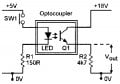
One important missing information in NCH tone generator output is "DC filter circuit or component". The audio output from the computer and android will have this DC filter circuit. The solution is in finding the circuit or the component, remove the same and connect the probes. All pre-amplifiers will have this filter for effective speaker performance. You can have a SPDT switch to select for filter or without filter. Anyhow our purpose is different , hence has to be removed or one can supply an external micro-current to the output probes, which is connected to the output with an DC filter circuit. Is it possible? I do not know. but known only to the learned members and hope they will be able to provide a solution please.
 

dheena0104

Joined Jul 10, 2019
36
Dear Mr Wayneh ji,
Greetings
Sorry for the delay. I was away from my town for some time due to unforeseen health problems.
Anyhow, time is running like anything, hence decided to put forward this update.
I bought one two channel PWM as shown in the attachment and ordered for two TLV271 ICs. Coupling these two as shown in fig will certainly help I think.
The only thing is random period wave as developed by Wayneh. In PWM unit, the appropriate IC is sealed under display, hence following Wayneh's method to create random period wave is hindered. Anyhow I will able complete the present project as soon as I am in receipt of the ordered ICs. Check for its functionality and will update.
I earnestly request Wayneh and other learned members for valuable feed backs please.
 

Attachments

dheena0104

Joined Jul 10, 2019
36
One minute thought
Kindly permit me to put forward the following observations to the learned members for further suggestions please.
Is it possible to use photo-transistor as shown in the attachment.
I tried with available one in LTspice LM358_AB. At lower frequencies (Wayneh circuit) worked nicely. Connected the output of the 555 IC directly to led and with R1 value of 10k, to the other side 100K for R2 with a load resistance parallel to R2 from 500 ohm to 100k. In put voltage at the transistor side 20V intead 18V. 100K load exhibited 20V and 200uA. 10K load 6.4V and 640uA. 1K load 0.7V and 700uA and 500 ohms load 0.350V and 750uA.
AT 1KHz frequncy current and voltage exhibited bi polar nature (+ve and -ve values). totally confused please
 

Attachments

Thread Starter

wayneh

Joined Sep 9, 2010
18,104
The only thing is random period wave as developed by Wayneh. In PWM unit, the appropriate IC is sealed under display, hence following Wayneh's method to create random period wave is hindered.
I suspect that changing the frequency is a very minor improvement and you can probably just omit it. The early, popular versions of these devices (I think they were called Voodoo boxes) had no such ability to randomize the frequency. The patented Alpha-Stim device includes the advance to randomize the frequency but that may have helped get the patent without delivering much of a real benefit. I'd go ahead and try your approach without it, and see if it works.
 

dheena0104

Joined Jul 10, 2019
36
Dear Mr Wayneh ji
Greetings
Thanks a lot for your kind suggestions; I will follow.
Is it possible to couple an opto transistor, for raising the applied voltage to 18V please. Any suggestions regarding compatible opto-transistor with frequency range from 1 Hz to 10 KHz and supply voltage 6V to 18V. It may take a month time to get the ordered TLV271, hence this request please; or I will try with LM358 in the mean time, I think!
Sorry for the novice requests and replies please.
Knowledge base: Kindly refer Novocure for Glioblastoma.
 

Thread Starter

wayneh

Joined Sep 9, 2010
18,104
Is it possible to couple an opto transistor, for raising the applied voltage to 18V please.
I'm not sure what you are asking. Are you wanting to increase the voltage applied to the user? I think you could use my existing design up to a voltage limited by the specifications of the ICs. You'd need more resistance to protect the LEDs and such but I think it would be easy to make these changes. I haven't actually looked it over yet.

I don't know how you'd achieve a controlled current using an optoisolator, and I don't really understand why you'd want the isolation.
 

dheena0104

Joined Jul 10, 2019
36
Dear Mr Wayneh ji,
Greetings
At the outset I request you to kindly bear with me for the novice questions. My aim is not for isolation but step up and step down like a transformer in an AC circuit (sorry, no prejudice; But only due to quriosity and learning please).
In the mean time I made some changes in the values of the circuit components as follows:
Out put from pin 3: changed 270k to 100 ohms directly connected (no flip flop IC) to lm358 (single unit). At the output pin of LM 358, added 14 k resistance, Which will be parallel to whatever body resistance it may be.
If the body resistance is 1K, the load resistance will be 14+1=15K. Now the current passing through 15K is 700uA and 11 V. If the body resistance is 100K, the load resistance will be 100+14k=114K. The current passing through the 114K load is 95uA and 11V. These are the LTspice stimulation values please. The abovalues are for 1 KHz Freq. When I tried for 0.5 Hz (your device circuit). I got same values but not to full X axis scale ( half scale) as exhibited by 1KHz Freq.
Kindly let me to have your suggestions please.
 

dheena0104

Joined Jul 10, 2019
36
u[date please
Everything works fine after removing randomizing circuit (555 with 470K and 47uF).
LTspice graphs for 0.5 Hz and 1KHz, load 115 K exhibited full scale graph.
Circuit components: Only one 555 to generate 0.5Hz, as described by Mr Wayneh and 1KHz as given in net (using 555) connected directly to single lm358 through 100 ohms resistor and 14K resistance in series to load (body resistance) at the out put of the lm358. No control is needed, I think please! kindly advice.
Now the small commercial PWM can be substituted for 555. All these are due to Mr Wayneh sincere efforts and suggestions.
Fine tuning and precautionary measure:
I am not having provision to check the substituted unit with an oscilloscope before applying as a therapeutic unit, hence earnestly request Mr wayneh's valuable suggestions and corrections after checking with the substituted commercial unit for NE555 please
 

dheena0104

Joined Jul 10, 2019
36
Update pl
Instead of 14K, 20K works better.
Some reports claim that body resistance between wrist and ankle is 1080 ohm through stimulation and 500 to 700 through measurements; Hence I changed the series resistance value from 14K to 20K with the following results for 555-lm358.
100/20K/500 ohms (body)-550uA/11V
100/20K/1K ohms (body)-480uA/11V
100/20K/10K ohms (body)-380uA/11V
100/20K/50K ohms (body)-160uA/11V
100/20K/100K ohms (body)-90uA/11V
I hope this will serve the pupose.
Commercial + TLV271 has to be checked for real world applications with Oscilloscope.
Thanking you
 

dheena0104

Joined Jul 10, 2019
36
Dear Mr Wayneh ji,
Greetings
Sure; I will send all appropriate things with schematics within two or three days because I am away from my town and will be able to reach back to my computer on or before 9th Feb 2020.
Sorry for the delay please.
 

dheena0104

Joined Jul 10, 2019
36
Dear Mr Wayneh ji
Greetings
Today I reached my town and trying to reach you through this reply. Your reply cautioned me about some mistakes in measurements, hence I rechecked the measuring points.
Earlier voltage measurements were before R6 instead before R3. (voltage will be divided by resistors in series-forgotten fact).
The measurements are as follows:
100/20K/500 ohms (body)-550uA/0.27V
100/20K/1K ohms (body)-480uA/0.525V
100/20K/10K ohms (body)-380uA/3.6V
100/20K/50K ohms (body)-160uA/8V
100/20K/100K ohms (body)-90uA/9V.
Kindly excuse me for the committed mistake please.
Circuit as shown below.
In the mean time I made some more observation with analogue multi-meter and stick electrode pads/
Provided small area kitchen towel wet pad In the middle of the stick pad to improve conductivity as shown in attachment.
One pad at the wrist and the other at the ankle.
Resistance was around 150 K-ohms average. Pads under moderate pressure exhibited 5 K-ohm.
Even though the measuring methodology seems not correct; what I felt was to provide identical environment like that of applying methodology will be appropriate to achieve desired results.
Kindly permit me to have your advice over this.
Optimum must be in between 75 K to 200 K or even between 50 K to 200 K, I think! If it is so by reducing 20 K to lower values one will be able to get good current and voltage.
 

Attachments

Thread Starter

wayneh

Joined Sep 9, 2010
18,104
Circuit as shown below.
I don't have the 555 or op-amp model you are using. Please include.

But looking at your file, I see R5 connects the output directly to an input. That won't work! My circuit uses that resistor as a shunt in series with the load and that gives a voltage proportional to the current.

What is the function of R6? It adds to the load impedance and that seems to work against you.
 

dheena0104

Joined Jul 10, 2019
36
Dear Mr Wayneh Ji
Greetings
I selectected the 555 timer from LTspiceXVII\lib\sym\zzz\timer. It says that it is an idealized timer module. I got this after typing 555 in the "open this micromodel's test fixtures". If I type NE555 I got differently labelled 555; With this NE555 the old circuit gave negative current and positive voltage at and before R6 respectively. R6 is assumed as body resistance (subject) and R5 to control current please.
The current at the resistance 300 ohms connected between input -ve and out put of LM358 exhibited bipolar nature (+ve and -ve).


1581394307324.png1581394362509.png
I am learning to use LTspice, hence do not know how to copy to this reply. Anyhow I have done something to show you the circuit and the graph after using NE555.
why this discrepancy please.
 

dheena0104

Joined Jul 10, 2019
36
Dear Mr Wayneh Ji,
Greetings
Earlier I was using windows 7 ultimate (genuine) for LTstimulation works. 10 days back I upgraded windows 7 to windows 10 (just before leaving my town).
Today I substituted NE555 with idealized timer module and checked. Simulation gave the same results as NE555. Totally confused. Moreover I am unable to retrieve the circuits, which I saved in windows 7 and sent to you through my earlier reply. Hence reinstalled LTspice in windows 10. Really a novice. Kindly bear with me please.
 

dheena0104

Joined Jul 10, 2019
36
Dear Mr Wayneh Ji,
Greetings
Now I learned a bit about line follower and OpAmp from your circuit for triangle wave out put. I have used the same circuit with a line follower and a comparator.
I got some results as I expected, but facing same problem as before in selecting 555 IC for wave generation.
If an idealized timer module (555) is used in the circuit as shown in the attachment, the resulting graph is to full scale (stop time 500s).
If NE555 is selected from the menu, the resulting graph stops at 450s as shown in the attachment.
I have downloaded the LTspice program from the company's website.
I am unable to copy and paste the circuits and appropriate graphs here (I do not know how to do it. Last time I attempted and due to that lost all saved files. Anyhow trying to learn from the failures), hence taken photographs of the same and uploading it for your valuable correction and guide lines pleasefull scale IC.jpgfull scale.jpgNE555 no full scale.jpgno full scale.jpg
 

dheena0104

Joined Jul 10, 2019
36
Dear Mr Wayneh Ji,
Greetings
One more update and correction please
When I increased the voltage divider resistance values to 100 k/100 k (as in your device), the graph is up to full stop time till 7.8 K load resistance and below that the graph is up to 1/2 stop time for NE 555 I C, but up to full scale with idealized 555 timer I C at various load resistance from 200 k to 1 k.
When the divider resistances are changed to 120 k/120 k. The graph is up to full stop time even for NE 555 at a load resistance varying from 200 k to 5 k.
The following values are for NE 555 (same for idealized 555 timer I C also):
Load 200 K (divider values 120 K/120 K) 40 uA at 7.0 V.
Load 10 K (divider values 120 K/120 K) 750 uA at 7.2 V.
Load 5 K (divider values 120 K/120 K) 1.6 mA at 8.0 V
Earlier attached circuit has different divider resistance value (91/22)
 

dheena0104

Joined Jul 10, 2019
36
Dear Mr Wayneh JI
Greetings
I feel extremely sorry for the inconvenience caused.
Being precise, I herewith request you to kindly let me to have your suggestions regarding amplifying voltage through BJT common base configuration for your circuit.
I tried one like that shown in the attachment. Simulation gave positive voltage and negative current at 5 K load.
1. Why the respective current wave was showing negative values even though voltage shows +ve values
Kindly let me to have a correct circuit diagram for voltage amplification (not current or current to lesser extent than voltage) through common base configuration or other means Pl. Your device helped a lot in some health conditions, hence this request for improving voltage, which may help me further.
BJT common base.jpg
 
Top