MIC1555 Sequential Timer - Triggers on Power Up?

Thread Starter

Slowmatch

Joined Jan 21, 2018
33
Hi All,

I have been trying to design a simple DC circuit that will give a half a second positive pulse 30-70 seconds after a momentary button is pressed.

The design context is a small free flight (ie non radio control) model aeroplane. The model climbs for 8 seconds on a timed motor run and then glides, but to prevent it flying away when it finds lift, it needs a 'De-thermaliser' (a.k.a. a DT.) This is some means of flipping up the tailplane to bring the model back down after a set time. There are mechanical options but I've been trying to create a electronic circuit to reduce the weight of the model.

The motor runs on a 200mAh one cell 3.7v Lipo, so I have sufficient power to run a 'spin off' micro coreless motor or to pulse a nichrome rubber band burner. The motor timer (my own design) is started by pressing a momentary switch which also provides a positive trigger for the DT circuit (the diagram also shows an independent start switch.) I am etching my own circuit boards and working with SMD parts down to about 0805 and SOT-23. Every fraction of a gram saved is important so a tight lay out and the smallest possible component count is helpful.

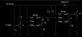
I've come up with the following sequential timer using two MIC1555 (SOT-23-5) chips https://uk.rs-online.com/web/p/timer-circuits/9101733. This is based on the standard double 555 circuit here: http://www.bowdenshobbycircuits.info/page9.htm#555-T.gif

This is working well but there is an issue: it triggers the burner pulse when attaching the battery ie on power up. This is just an immediate second stage pulse - ie no delay. This is obviously not ideal with a nichrome burner! Please can anyone suggest a way of preventing this or point to something I may have missed? The MIC1555 does not have a RESET pin like the standard 555 so I'm not quite sure what is happening.

If I can solve this power up triggering I have a functional circuit. But I'd also be interested to hear if there are simpler ways to achieve the same result - especially with fewer components.

Thanks in advance!

Jon
 

Attachments

sghioto

Joined Dec 31, 2017
5,380
I haven't fully analyzed the circuit but try adding a 100K resistor from the gate of Q2 to ground.
EDIT: Another problem is the second MIC1555 is activated by a falling edge trigger. When power is first applied the output of the first chip is low causing the the second MIC1555 to trigger instantly.
 
Last edited:

Thread Starter

Slowmatch

Joined Jan 21, 2018
33
Thanks for the reply.

I haven't fully analyzed the circuit but try adding a 100K resistor from the gate of Q2 to ground.
This was something I tried as I wondered if the gate was floating but it doesn't make any difference. I think the gate is held low by the Trigger pin anyway.


EDIT: Another problem is the second MIC1555 is activated by a falling edge trigger. When power is first applied the output of the first chip is low causing the the second MIC1555 to trigger instantly.
The second chip is definitely triggering and running through the second stage monostable pulse on power up.

This doesn't happen to a single MIC1555 monostable though, or the first stage? I thought it needed a falling edge to trigger?
 

AnalogKid

Joined Aug 1, 2013
10,987
Not a falling edge. The inputs to a 555 go to analog comparators, so they are level-sensitive, not edge-sensitive. If the Trigger input is below 0.33 x Vcc, the 555 wakes up in the triggered state: output is high, and the timing capacitor C2 is being charged up.

Also, it looks like R2-C2 time out at a little under 50 ms, not 500 ms.

ak
 

sghioto

Joined Dec 31, 2017
5,380
CS line is a CHIP SELECT/ RESET but not available on the model 1555 the TS is using as far as I can tell.
One solution is to inhibit the output of IC2 using Q3 when first powering up.
1635100067935.png
 

AnalogKid

Joined Aug 1, 2013
10,987
Does the DT signal have to be positive-going?

Either way, this can be done by replacing the two 555's with a single CD4093. One gate is an output pulse disabler with its own R-C timer. This suppresses an output signal while the 0.5 s timing capacitor stabilizes. The total circuit would have fewer pins. The tradeoff is that the circuit output is disabled for a couple of seconds after power-on.

Your circuit should have a power supply decoupling capacitor for each 555. When you add in these, the alternate circuit might be smaller.

Not my favorite option, but -- nothing will be smaller and lighter weight than an 8-pin PIC. Input signal > PIC > Q2. Done.

https://ww1.microchip.com/downloads/en/DeviceDoc/40001239F.pdf

ak
 
Last edited:

Thread Starter

Slowmatch

Joined Jan 21, 2018
33
Not a falling edge. The inputs to a 555 go to analog comparators, so they are level-sensitive, not edge-sensitive. If the Trigger input is below 0.33 x Vcc, the 555 wakes up in the triggered state: output is high, and the timing capacitor C2 is being charged up.
Ah ok, that makes more sense now, thank you. I misunderstood the Bowden page when it said: " The second 555 stage will not respond to the rising voltage since it requires a negative, falling voltage at pin 2, and so the second stage output remains low and the relay remains de-energized." It hadn't clicked that said pin was already high - except during power up.


Also, it looks like R2-C2 time out at a little under 50 ms, not 500 ms.
The timing is not that critical - just enough to burn a rubber band through but not melt the nichrome. It's working with these values anyway...
 

Thread Starter

Slowmatch

Joined Jan 21, 2018
33
If you are not using the CS line, perhaps you could place a RC network on this pin to pull it low during powerup.
As stated the MIC1555 doesn't have a CS or RESET pin. The MIC1557 does but I believe that is intended for Astable use.

I do have a couple of TLC555CDR (SOIC 8) chips here with the usual outputs - I could possibly use one for the second stage?
 
Last edited:

Thread Starter

Slowmatch

Joined Jan 21, 2018
33
CS line is a CHIP SELECT/ RESET but not available on the model 1555 the TS is using as far as I can tell.
One solution is to inhibit the output of IC2 using Q3 when first powering up.
View attachment 251005
Thank you for this - clever stuff. But it does bump up the parts count and board space somewhat.

The datasheet says that the threshold pin has precedence over the trigger pin, forcing output low when THR is high. So I wondered if there may be some way to keep THR high during power up instead?
 

sghioto

Joined Dec 31, 2017
5,380
Using the 555 for the second stage will work. Connect a capacitor from the reset pin to ground. Will probably need to experiment with the value, start with a 100nf.
 

Thread Starter

Slowmatch

Joined Jan 21, 2018
33
Does the DT signal have to be positive-going?
It's just the way the motor timer output is configured - I might be able to re work it. It's started with a momentary switch from the Lipo + via one half of a BAT54A Schottky diode.

One other consideration is that the little drone motor is rather an amp hog and the voltage drops to about 2.7V under load. It doesn't seem to affect the timing of the first stage delay but it might be a consideration in other design ideas.


Either way, this can be done by replacing the two 555's with a single CD4093. One gate is an output pulse disabler with its own R-C timer. This suppresses an output signal while the 0.5 s timing capacitor stabilizes. The total circuit would have fewer pins. The tradeoff is that the circuit output is disabled for a couple of seconds after power-on.
....
Not my favorite option, but -- nothing will be smaller and lighter weight than an 8-pin PIC. Input signal > PIC > Q2. Done.
I'm very open to other ways to skin this particular cat, especially anything that gets the weight and footprint down. Using a microcontroller is something I've looked into looking into (as it were) but it would require a large investment of time for me to learn - I'm a total rookie. There are a handful of cottage suppliers making Dethermalizers that use Microcontrollers but they often have fiddly "count the LED flashes" type programming which is a right faff on a sunny flying field. I quite like the idea of a single trimmer and a tiny screwdriver.


Your circuit should have a power supply decoupling capacitor for each 555. When you add in these, the alternate circuit might be smaller.
Would you mind suggesting values and showing me where these should go please? I am as you can probably tell a hobbyist who has a lot to learn!


Thank you for all the responses and interest.

Jon
 

AnalogKid

Joined Aug 1, 2013
10,987
Power supply decoupling capacitors - one for each + and each - power pin on each IC. For logic ICs, that usually is one per part. Opamps in dual-supply circuits need two. Each cap goes from the power pin to a GND pin, as close as possible to the pins, with the shortest possible leads or traces. 0.1 uF ceramic is the standard part for almost everything, but there are exceptions. If the 555 were switching the load directly, I'd recommend something in the 1.0 uF to 2.2 uF range to compensate the larger current spikes.

ak
 

AnalogKid

Joined Aug 1, 2013
10,987
First pass. This might look more complex than the original 555 circuit, but it isn't. It does include a POR (power-on reset) circuit (R1-C1) that eliminates the errant output pulse without needing a multi-second stabilization period.

Not counting the input switch and resistor, and adding in two decoupling capacitors, the original circuit has 41 pins versus 38 here. I've found that pin count is a fair measure when comparing the complexities of hand-assembled circuits.

R2-R3-C2 are the long, adjustable delay. D1 resets the capacitor quickly.

R4-C3 are the short output pulse former. The FET's threshold voltage and gain act as a comparator, producing a pseudo-square output pulse. If the load is a DC motor, best to include a 1N4004 suppression diode across it.

U1A-U1B form a set-reset flipflop that latches the input signal and drives the timer. Thus, the input signal does not have to stay high for the whole 70 seconds.

Because this circuit has a latch and pulse-former instead of a true monostable, it does not automatically reset itself. To reset the circuit for another cycle, either cycle the power or add a pushbutton switch across C1.

The four gates are interchangeable, and can be reassigned to ease pcb layout trace routing.

ak

Pulse-Delay-2-c.gif
 

crutschow

Joined Mar 14, 2008
34,285
Below is the LTspice simulation of AK's basic circuit with a few modifications:

R3 and R5 prevent excess current into the IC inputs from the capacitors if power is suddenly removed.

Edits:
Second Modification below:

Removed added diode D2, and instead moved R2's connection to the drain of the MOSFET to provide the reset function and generate the output pulse width.

The operation is as follows:
At power-up, R2-C2 sets the U1a-U1c latch (red trace) to its reset state (output transistor off).
The input pulse (green trace) flips the state of the U1a-U1c latch.
This starts to pull C1 low through R1 (blue trace)
When C1's voltage reaches the threshold voltage of U1d, its output goes high, turning on the MOSFET (yellow trace).
This low voltage at M1's drain also resets the latch through R2, causing U1a's output voltage to go back high.
This then raises C1's output voltage through D1, causing U1d's output voltage to go back low, turning off the MOSFET.
The value of R2 and C2 determines the time it takes U1a's output to reset high, and thus the output pulse width.

Note that the MOSFET must be a logic-level type MOSFET (max Vgs(th) <2V).


1635214388183.png
 
Last edited:
Top