Facebook
 Google
 GitHub
 Linkedin
Hello,
Read this:
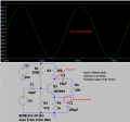
Emitter-Bias
Inserting a resistor RE in the emitter circuit as in figure below causes degeneration, also known as negative feedback. This opposes a change in emitter current IE due to temperature changes, resistor tolerances, beta variation, or power supply tolerance. Typical tolerances are as follows: resistor— 5%, beta— 100-300, power supply— 5%. Why might the emitter resistor stabilize a change in current? The polarity of the voltage drop across RE is due to the collector battery VCC. The end of the resistor closest to the (-) battery terminal is (-), the end closest to the (+) terminal it (+). Note that the (-) end of RE is connected via VBB battery and RB to the base. Any increase in current flow through RE will increase the magnitude of negative voltage applied to the base circuit, decreasing the base current, decreasing the emitter current. This decreasing emitter current partially compensates the original increase.

Emitter-bias
Note that base-bias battery VBB is used instead of VCC to bias the base in the figure above. Later we will show that the emitter-bias is more effective with a lower base bias battery. Meanwhile, we write a KVL equation for the loop through the base-emitter circuit, paying attention to the polarity on the components. We substitute IB≅IE/β and solve for emitter current IE. This equation can be solved for RB, equation: RB emitter-bias, Figure above.
Before applying the equations: RB emitter-bias and IE emitter-bias, the figure above, we need to choose values for RC and RE. RC is related to the collector supply VCC and the desired collector current IC which we assume is approximately the emitter current IE.
Normally the bias point for VC is set to half of VCC. Though, it could be set higher to compensate for the voltage drop across the emitter resistor RE. The collector current is whatever we require or choose. It could range from micro-Amps to Amps depending on the application and transistor rating. We choose IC = 1mA, typical of a small-signal transistor circuit.
This comes from this page of the eBook:
https://www.allaboutcircuits.com/textbook/semiconductors/chpt-4/biasing-calculations/
Bertus
Read this:
Emitter-Bias
Inserting a resistor RE in the emitter circuit as in figure below causes degeneration, also known as negative feedback. This opposes a change in emitter current IE due to temperature changes, resistor tolerances, beta variation, or power supply tolerance. Typical tolerances are as follows: resistor— 5%, beta— 100-300, power supply— 5%. Why might the emitter resistor stabilize a change in current? The polarity of the voltage drop across RE is due to the collector battery VCC. The end of the resistor closest to the (-) battery terminal is (-), the end closest to the (+) terminal it (+). Note that the (-) end of RE is connected via VBB battery and RB to the base. Any increase in current flow through RE will increase the magnitude of negative voltage applied to the base circuit, decreasing the base current, decreasing the emitter current. This decreasing emitter current partially compensates the original increase.
Emitter-bias
Note that base-bias battery VBB is used instead of VCC to bias the base in the figure above. Later we will show that the emitter-bias is more effective with a lower base bias battery. Meanwhile, we write a KVL equation for the loop through the base-emitter circuit, paying attention to the polarity on the components. We substitute IB≅IE/β and solve for emitter current IE. This equation can be solved for RB, equation: RB emitter-bias, Figure above.
Before applying the equations: RB emitter-bias and IE emitter-bias, the figure above, we need to choose values for RC and RE. RC is related to the collector supply VCC and the desired collector current IC which we assume is approximately the emitter current IE.
Normally the bias point for VC is set to half of VCC. Though, it could be set higher to compensate for the voltage drop across the emitter resistor RE. The collector current is whatever we require or choose. It could range from micro-Amps to Amps depending on the application and transistor rating. We choose IC = 1mA, typical of a small-signal transistor circuit.
This comes from this page of the eBook:
https://www.allaboutcircuits.com/textbook/semiconductors/chpt-4/biasing-calculations/
Bertus