Measuring Microcurrent over a Transformer with Arduino

Thread Starter

danielantonic

Joined Sep 22, 2019
68
Hello again. I'm getting back into this project, and I have made a bit of progress:
  • I have a LiPo power source that will supply 5V constantly (for Raspberry Pi). I don't need the optocouplers etc. now, and I also want to keep the majority of the circuitry working on 5V to keep things simple.
  • I made a 30V boost converter using an LM2577 to supply the 30V from a 5V source (not sure how stable it is as yet - haven't stress tested it)
  • I have some MCP6004 Op Amps (5V rail to rail) and the 55V MOSFETs (went with 55V in case I decide to up the voltage from 30 at some point)

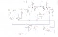
I designed an H-bridge and constant current circuit (attached) that seems to meet my needs. A few notes on the components:
  1. EN_1 and EN_2 will be 5V logic from the Arduino. Via R8, R9, Q3 and Q4, these 'enable' signals change the direction of the current flow through the electrodes (or stop current flow if needed) by disabling/enabling the correct OP Amp and via R1-R6 along with Q1 and Q2, the correct MOSFET pairs
  2. The DAC is an MPC4725 0-5V output
  3. R11 is to limit the maximum current drawn through the electrodes
  4. R7 and R10 are to stop any accidental short circuit

I have run a simulation of the circuit and it seems plausible, but I'm sure the resistor values are off, and I probably need some caps somewhere. So far the only things that I have specs for are the MOSFETS and OP AMPS - the transistors can be changed/removed - I simply need a way of controlling the MOSFETS with 5V signal.
 

Attachments

Irving

Joined Jan 30, 2016
5,139
Having two active threads on the same topic isn't allowed under forum rules - sooner or later a moderator will lock one down so best to choose one and stick with it.

Notwithstanding that, the comments made by myself and others on the other thread re this design still apply. In particular Q3/Q4 won't work the way you're expecting them to do.
 

Thread Starter

danielantonic

Joined Sep 22, 2019
68
Having two active threads on the same topic isn't allowed under forum rules - sooner or later a moderator will lock one down so best to choose one and stick with it.

Notwithstanding that, the comments made by myself and others on the other thread re this design still apply. In particular Q3/Q4 won't work the way you're expecting them to do.
Fair enough - the other thread was initially just going to be about the op amp side of things, but I'll stick to here :)

Without the transistors, what should I do to activate the H-bridge? In the design you suggested using optocouplers, but I thought they were just for isolation (which isn't needed now its a battery design). Keep in mind that I want to limit the current and be able to switch directions :)
 

Irving

Joined Jan 30, 2016
5,139
The upper transistors Q1 & Q2 are fine, but you need to sort out the resistor values, try R1, R2 = 10k & R3, R4 = 22k for 30v or 51k for 60v.

The bigger problem is that when the top MOSFET turns on you get a big (10mA+) current spike from the lower CC generator on that side due to the sudden rise in voltage at its drain, coupled with the gate-source 'turn-on' current from the top MOSFET. The loop response of the CC generator simply can't respond fast enough to shut it down. So before turning on the top MOSFET you need to isolate the lower CC generator on that side completely. Turning off the DAC feed to the opamp as you show is not an option as all that does is allow the opamp output & therefore the gate voltage to float up to the opamp supply voltage - exactly the opposite of what's needed.

You need to consider ways to either ground both electrodes to remove the spike or short them together to bypass them. Or slow the rise time of the drive to the upper MOSFET to reduce the spike though I suspect it may then be too slow to meet other criteria.

Incidentally, when simulating this you must have are representative load between the electrodes else the simulation is invalid. I don't see the point of the 13k5 resistors, its just wasting compliance voltage.
 
Last edited:

Thread Starter

danielantonic

Joined Sep 22, 2019
68
So before turning on the top MOSFET you need to isolate the lower CC generator on that side completely. Turning off the DAC feed to the opamp as you show is not an option as all that does is allow the opamp output & therefore the gate voltage to float up to the opamp supply voltage - exactly the opposite of what's needed.

You need to consider ways to either ground both electrodes to remove the spike or short them together to bypass them. Or slow the rise time of the drive to the upper MOSFET to reduce the spike though I suspect it may then be too slow to meet other criteria.
Thank you very much - I think I understand what you mean. Would putting optocouplers between the op amp and gates still allow the current to be constant (just take resistance of the phototransistors into consideration)? NB - I have redone the schematic and re-designated components to make it easier to follow.

1640328891302.png
Incidentally, when simulating this you must have are representative load between the electrodes else the simulation is invalid. I don't see the point of the 13k5 resistors, its just wasting compliance voltage.
Long term, there are going to be 5 of these set up (5 channels), so the extra resistors in series with the electrodes are just to prevent human error/short circuits between channels.
 
Last edited:

Irving

Joined Jan 30, 2016
5,139
No that wont work. Please try to keep the component numbering the same from iteration to iteration; its extremely tedious to have to keep refering back to previous drawings and/or keep ours in sync with yours. What package are you using?

In your new drawing, you cannot gate the DAC signal with Q1 and Q2 like that. Transistors dont work that way. In any case the DAC signal is an analogue voltage so wont activate the digital control of Q3 and Q4 as you intend. These have to be completely separate but linked circuits. Also timing is critical to avoid the spikes i mentioned in my last post. The gating/control of the DAC has different timing requirements to the activation of Q3 and Q4.

You cannot use optocouplers that way. A 'turned on' transistor in an optocoupler has a limited operational range of current entirely defined by the LED current and is highly non-linear. Your constant current generation will be anything but constant... A proper analogue switch might work but the voltage range there is probably too large for most.

I think your design has some very fundamental issues. In fact, having played around for a couple of hours with the simulator, I'm fairly convinced a different approach might be needed...
 

Thread Starter

danielantonic

Joined Sep 22, 2019
68
Thanks for the feedback - I'll keep the numbering the way it is

I'm using TinyCad for the schematic, but testing parts in the Circuit simulator here: https://www.falstad.com/circuit/

I was having a look at your idea back in post 36. I'm a bit confused as to how the op amps U4 and U5 interact with U3. Will the photodiode in U3 conduct if either of the LEDs are activated? I haven't come across them before and haven't got one in the simulator to try.

Here's an idea how it could be done - Q1 - Q4 create an H-bridge. If Q1 is on through DRV_Phase1 being logic1, DAC_IN sets the current waveform into electrode1 and a logic1 on EN_Phase1 grounds electrode2 through Q4. Similarly DRV_Phase2 and EN_Phase2 apply the DAC_IN set current to electrode2 via Q2 with electrode1 grounded through Q3, thus providing the reverse polarity. Turning both DRV_ inputs 'off' and setting both EN_ inputs 'on' grounds both electrodes as the 'safe' position.

View attachment 244477
 

Irving

Joined Jan 30, 2016
5,139
No the optocoupler at U3 is a special type. Its 1 LED and two matched photodiodes. With U4 driving the LED and monitoring the feedback current from 1 diode and using the other diode as the input to U5 we can be sure the output of U5 tracks the output of U4 but is fully isolated from it. You probably won't find a model for it in your simulator but you can probably pull one in from somewhere assuming it allows normal Spice models. I've not run a simulation with that arrangement so can't be sure if it doesn't suffer from the same issues. I've not used your simulator but i know these sorts of transient switching issues don't appear in many 'low-end' simulators; that one appears to be nowhere near the sophistication of LTSpice...
 

Thread Starter

danielantonic

Joined Sep 22, 2019
68
Ok, well that settles it - I need to learn how to use LT Spice... I wanted something to do over the holidays anyway ;-)

Thanks again for your help Irving. I'll play with some proper simulations and post my results here :)
 

Thread Starter

danielantonic

Joined Sep 22, 2019
68
Hello again. I just had a brain wave - instead of trying to interface with the higher voltage circuit, all I want to do is control the current through the H-Bridge... so why not control it from the sources of the bottom MOSFETs? I came up with this design - changes from the old are removing R7 and R8, adding an extra MOSFET to limit the current through the entire H-Bridge. The Op Amp is just a buffer. Using 8.2k on R11 allows 550uA across the electrodes with a 10k load according to my simulations.

1640509975958.png
 

Irving

Joined Jan 30, 2016
5,139
Well that sort of works, but I think there may be a few problems...

For starters the 13.5k resistors significantly reduce the voltage at the electrodes to the point where the whole circuit is compromised.... What shorted to what do you think is an issue? Anyway, I've set them to 1ohm for now. Next, the low currents mean that the dynamic impedance of the CC generator and lower MOSFETs are each about 50kOhm, ie the source voltage V(vs) of the lower MOSFET switches rises to 8 or 9v with a gate voltage of 10v - they are barely turned on. This isn't good for stability.

Load = 5k
1640618382880.png


Load = 50k
1640618451001.png
 

Thread Starter

danielantonic

Joined Sep 22, 2019
68
There are going to be 5 of these circuits in parallel with different currents set (individual channels) The resistors were to prevent one channel connecting to another if the user places the electrodes incorrectly, accidentally touches an electrode to a grounded object etc. 13.5k was just a random value I chose so it can be anything.

I also had R9 and R10 at 10k not 1k (simply because I have a ton of 1% 10ks at my disposal). I figured I just needed a 1:2.2 ratio with R1:R3 and R2:R4, so went with values to use what I had on hand.

Since the current is so low, is some sort of amplification needed to stabilise the bottom MOSFETs?
 

Thread Starter

danielantonic

Joined Sep 22, 2019
68
Well I just did some tests using 10k for all resistors and this design is matching my simulations!

A 0-5V pulsed DC signal goes through the buffer U1B, is attenuated by the MCP4134 digital potentiometer, buffered again by U1A and this sets the max current flowing through the H Bridge (the frequency of this signal is the key to FSM treatment)

The last part that I'm not 100% sure about is keeping the channels galvinically isolated. I was thinking of a 1:1 transformer at the electrodes to mirror the voltage/current of the H-bridge. Would this work? The frequency range is 10-10khz.

1640840138449.png
 

Irving

Joined Jan 30, 2016
5,139
U1A -ve input should connect to the top of 11/pin 3 FET5

I doubt the transformer output will be consistent enough across load, frequency and current variations... inductive load on the bridge could be problematic
 
Top