Measuring LED forward voltage

WBahn

Joined Mar 31, 2012
32,848
Also, can you tell me if the way i think is correct in the previous message? :eek: Hm.. Yeah seems clear that Vac should be 3V, not +21V, but i understand it in the other way.. If we place the positive multimeter lead to the positive battery terminal, we get positive voltage ( in this caes +12V) , and if we take other multimeter lead ( the black one ) and measure also the positive voltage on Vc, we are gonna get negative voltage, so -9V, so Vac we get +12-9=+3V?
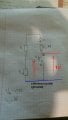
If you place the positive lead on the positive terminal of a 12V battery, it will measure +12V ONLY IF the negative lead of the multimeter is placed on the negative terminal of the battery (or some other point that is at that same potential).

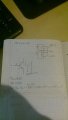
The voltage at a point, say Va, is, by definition, the voltage at that point relative to some reference. In order to work in any meaningful way with voltages at different points, those voltages have to be measured relative to the same reference. Now, it is not necessary for us to ever know what that reference is, as long as it is always the same for all of our work. Thus we can take voltage difference measurements and work with those. But any time we want to say that the voltage at a point is a certain value, we need to establish what the common reference is that is used for all such values.
 

Thread Starter

zazas321

Joined Nov 29, 2015
936
Okay, so as i understood, the reference point must be same, for all circuit measurements...But have a look at the picture. We can measure Vc and Vb taking ground as reference point.. But if we have to measure Vcb or Vbc , the ground cannot be the reference point .. So if we calculated Vbc or Vcb = Vc-Vb=0,3V. So how do i know now from which point measured we actually get 0,3V? Vcb or Vbc?
 

Attachments

WBahn

Joined Mar 31, 2012
32,848
Let's say that you choose some point G in the circuit and declare that it's voltage is going to be -3.4 V for some inexplicable reason. You know measure the voltage at node A (relative to G) and get -6.8 V. You now measure the voltage at node B (again, relative to G) and get +2.2 V. What result would you have gotten had you just measured node B relative to node A? Let's do the math.

Vag = Va - Vg = -6.8 V
Vbg = Vb - Vg = +2.2 V

Vba = Vb - Va = (Vb - Vg) - (Va - Vg) = Vbg - Vag = (+2.2 V) - (-6.8 V) = 9 V.

Absolutely nothing would have changed with that final result had we chosen to use the voltage at node N as our reference and declare that it's voltage is +1234.567 V.
 

WBahn

Joined Mar 31, 2012
32,848
Okay, so as i understood, the reference point must be same, for all circuit measurements...But have a look at the picture. We can measure Vc and Vb taking ground as reference point.. But if we have to measure Vcb or Vbc , the ground cannot be the reference point .. So if we calculated Vbc or Vcb = Vc-Vb=0,3V. So how do i know now from which point measured we actually get 0,3V? Vcb or Vbc?
Vc = 1 V
Vb = 0.7 V

Vcb = Vc - Vb = 1 V - 0.7 V = 0.3V
Vbc = Vb - Vc = 0.7 V - 1 V = -0.3 V

Vpn means the voltage difference between Vp and Vn. It also means the amount by which the voltage at node P exceeds the voltage at node N.

When you take a voltage measurement with a typical voltmeter, what it displays is Vpn where node P is the node connected to the positive lead and node N is the node connected to the negative lead.
 

Thread Starter

zazas321

Joined Nov 29, 2015
936
Yeah thanks, finаlly i got this ! :) . I would like to get back to discussion about transistors. If we remove a diode at the base( i just use an arrow to make it clear that we need some current flowing in to the base to turn transistor ON) , so when the transistor is ON, it can have 2 modes: saturation and amplification.. The difference is the junction CB forward or reverse biased, but why i cannot mark this junction as a diode? :/
 

Attachments

WBahn

Joined Mar 31, 2012
32,848
What do you mean "mark this junction as a diode"? The diode-like symbol used in the emitter leg of the transistor symbol does not mean that there is a diode in that leg and not the other. It is merely a means of identifying the emitter pin of a BJT transistor. They could have indicated it with an 'x' or a dot or some other way.
 

Thread Starter

zazas321

Joined Nov 29, 2015
936
Yeah , thats what im asking, hmm yeahh. But when the CB junction is reverse biased , the current flows from collector to base, and when its forward biased, it flows from base to collector. Am i right there?
 

Jony130

Joined Feb 17, 2009
5,598
No, You are totally wrong. As I said early do not treat BJT as a two separate diodes.
Base- emitter junction act just like a ordinary diode. But CB junction not. In active region Base-Collector junction is reverse biased. So no current flow between base and collector. Instead the current will flow from Collector to Emitter. And the Base current will also flow from Base to Emitter. And this is why Ie = Ib + Ic.
 

WBahn

Joined Mar 31, 2012
32,848
Yeah , thats what im asking, hmm yeahh. But when the CB junction is reverse biased , the current flows from collector to base, and when its forward biased, it flows from base to collector. Am i right there?
When the CB junction is reverse biased, their would normally be no current flowing. However, the injection of charge carriers into the base region (electrons or holes depending on the transistor type) provides a mechanism for current to flow through the reverse-biased junction. Do not try to think of a transistor as being two junction diodes placed back to back. This is NOT what a transistor is and this treatment can't capture what is going on.

Even when the base-collector junction is forward biased, as it is in saturation, the current still flows in the reverse direction (as long as the collector voltage exceeds the emitter voltage (talking NPN here) by enough to get current to flow, about a quarter volt or less).
 

Thread Starter

zazas321

Joined Nov 29, 2015
936
So you basically mean even if the CB junction is forward biased, that doesnt mean that the current flows from + to -?

No, You are totally wrong. As I said early do not treat BJT as a two separate diodes.
Base- emitter junction act just like a ordinary diode. But CB junction not. In active region Base-Collector junction is reverse biased. So no current flow between base and collector. Instead the current will flow from Collector to Emitter. And the Base current will also flow from Base to Emitter. And this is why Ie = Ib + Ic.
Yeah, got it. But how does exactly current flows when its saturated? Its the same as the linear mode? current will flow from collector to emmiter and from base to emmiter , but they will have maximum values?
 

WBahn

Joined Mar 31, 2012
32,848
So you basically mean even if the CB junction is forward biased, that doesnt mean that the current flows from + to -?
There are two "+ to -" at play. When the CB junction is forward biased (again, using an NPN as the model for discussion) the base is more positive than the collector -- but by less than a diode drop so it still is not "on". But the collector is still positive relative to the emitter and the collector current is flowing from collector to emitter.

Yeah, got it. But how does exactly current flows when its saturated? Its the same as the linear mode? current will flow from collector to emmiter and from base to emmiter , but they will have maximum values?
In the active (linear) mode, think of it this (admittedly sloppy) way: each element of charge that enters the base region (via the base connection) creates an environment in that region that permits many (as in hundreds) of charges to sweep through between the collector and the emitter. As you pump more and more charge via the base connection, the effectiveness of each charge becomes less and less. This is a continual process, but at some point each base charge injection only allows ten units of charge to flow between collector and emitter. At this point, purely by convention (for small signal transistors, not power transistors) we declare the base region to be "saturated".
 

dl324

Joined Mar 30, 2015
18,329
If we remove a diode at the base( i just use an arrow to make it clear that we need some current flowing in to the base to turn transistor ON) , so when the transistor is ON, it can have 2 modes: saturation and amplification.. The difference is the junction CB forward or reverse biased, but why i cannot mark this junction as a diode? :/
You are misusing the diode illustration I used to help you visualize the junctions when you were trying to use KVL. Then you started drawing it incorrectly and using it inappropriately.
 

Thread Starter

zazas321

Joined Nov 29, 2015
936
There are two "+ to -" at play. When the CB junction is forward biased (again, using an NPN as the model for discussion) the base is more positive than the collector -- but by less than a diode drop so it still is not "on". But the collector is still positive relative to the emitter and the collector current is flowing from collector to emitter.

Ok, i will try to ilustrate what u have said there , and see if i understood. So in the first picture i tryed to draw some circuits. For example if we have Vce ( collecttor relative to emmiter) = +0,2V, while the Base is more positive than collector by +0,5V... I would say that the higher voltage "wins" and the current will flow at the higher voltage different, so according to my calculations it should flow from base to collector, but you have said that it flows from Collector to emitter. I have underlined the place that i cant understand... I have seen many pictures and i understand that when the current flows through base to emmiter it "opens" a way the current to easily flow from emitter to base, but my calculations somehow show that there is a positive voltage between Base and collector that makes electrons to flow from base to collector..


In the active (linear) mode, think of it this (admittedly sloppy) way: each element of charge that enters the base region (via the base connection) creates an environment in that region that permits many (as in hundreds) of charges to sweep through between the collector and the emitter. As you pump more and more charge via the base connection, the effectiveness of each charge becomes less and less. This is a continual process, but at some point each base charge injection only allows ten units of charge to flow between collector and emitter. At this point, purely by convention (for small signal transistors, not power transistors) we declare the base region to be "saturated".
So u basically say that in linear mode the little current through BE makes huge difference at CE, but as the current increases the difference is getting lower and lower , till we "hit" the highest points where the increasing BE current cant change CE because its already in its maximum stage?
 

WBahn

Joined Mar 31, 2012
32,848
So u basically say that in linear mode the little current through BE makes huge difference at CE, but as the current increases the difference is getting lower and lower , till we "hit" the highest points where the increasing BE current cant change CE because its already in its maximum stage?
That's not too bad a way of thinking about it.
 

Thread Starter

zazas321

Joined Nov 29, 2015
936
There are two "+ to -" at play. When the CB junction is forward biased (again, using an NPN as the model for discussion) the base is more positive than the collector -- but by less than a diode drop so it still is not "on". But the collector is still positive relative to the emitter and the collector current is flowing from collector to emitter.

Ok. So talking about this part now. I have underlined a place where im not sure what means and also im adding a picture.. So we have Collector more positive than emmiter, and we have collector less positive than base, so how do we know which voltage is the leading one? So lets say we have Vce = 0,2V and we have Vbc=0,5V, Vbc is higher than Vce, so maybe it should "win" and dictate the current flow?
 

Attachments

WBahn

Joined Mar 31, 2012
32,848
You are still trying to think of a transistor as being two distinct diodes. It isn't.

But even if it were, you would get very little flow (and it would be from base to collector -- in an NPN) with a forward bias of 0.5V (it would be more than three orders of magnitude less than the base-emitter current).
 

WBahn

Joined Mar 31, 2012
32,848
But in any electronical circuit current flows from + to -, aint that rightt?
In a word, no. Remember that current flows in a circuit and that all of the voltages must sum to zero around that circuit. Hence, if current is flowing from + to - in one part of the circuit, it must be flowing from - to + in some other part. In the former case energy is being converted from electrical to some other kind and in the latter energy is being converted from some other kind to electrical.
 
Top