Facebook
 Google
 GitHub
 Linkedin
Hello
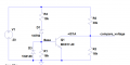
I have the case where the collector base current on a npn transistor could be negative. I know, the path between base and collector feels like a diode. So there will be a voltage of about 0.5V, but I don't find any data which current is allowed thrugh this diode path. Does anyone has an idea (e.g. for BC846)?
I have the case where the collector base current on a npn transistor could be negative. I know, the path between base and collector feels like a diode. So there will be a voltage of about 0.5V, but I don't find any data which current is allowed thrugh this diode path. Does anyone has an idea (e.g. for BC846)?