LTSPICE undefined subcircuit error

Thread Starter

Merchant

Joined Aug 10, 2017
3
I downloaded the P-SPICE simulation model for the NCP5183: High Voltage 4.3 A High and Low Side Driver (http://www.onsemi.com/PowerSolutions/product.do?id=NCP5183) and used the .lib file to create the model for it using these instructions: http://www.linear.com/solutions/4678. But when I add it to my LTspice schematic and try to simulate it I get the following error: 'Undefined subcircuit: rsffpc_abm'.

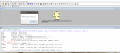
Can anyone else please download this model and attempt to get it working in LTspice? I'm clueless at this point. I've attached the pspice sim file and a screenshot of the error.

Thanks very much
 

Attachments

eetech00

Joined Jun 8, 2013
3,858
HI

The spice model from OnSemi is bad. There is no subcircuit named "RSFFPC_ABM" but there are three statements in the .lib file that call "RSFFPC_ABM". The spice "glue" is X_U1, X_U3, X_U4 and X_U6.

You should notify OnSemi that the model is incomplete.
 

Thread Starter

Merchant

Joined Aug 10, 2017
3
HI

The spice model from OnSemi is bad. There is no subcircuit named "RSFFPC_ABM" but there are three statements in the .lib file that call "RSFFPC_ABM". The spice "glue" is X_U1, X_U3, X_U4 and X_U6.

You should notify OnSemi that the model is incomplete.
Thanks for the reply. I’ll let them know.
 

sunsetb

Joined Apr 11, 2017
3
Actually, the RSFFPC_ABM refers to a standart PSPICE flip flop
Here a link to the Pspice standart component http://www.pspice.com/logic/flip-flops?page=6
The thing is, it should be automatically understood by LTSPICE, but it seems that... well LTSPICE doesn't know the standart component.
I know that SIMETRIX does, but it isn't freeware. And it tends to bug a lot (the version 8.00 I had used to crash mysteriously with certain component...)

Well well, if i have a better answer the coming days, I will let you know
 

eetech00

Joined Jun 8, 2013
3,858
Actually, the RSFFPC_ABM refers to a standart PSPICE flip flop
Here a link to the Pspice standart component http://www.pspice.com/logic/flip-flops?page=6
The thing is, it should be automatically understood by LTSPICE, but it seems that... well LTSPICE doesn't know the standart component.
I know that SIMETRIX does, but it isn't freeware. And it tends to bug a lot (the version 8.00 I had used to crash mysteriously with certain component...)

Well well, if i have a better answer the coming days, I will let you know
Hi

LTspice is "sorta" pspice compatible. :cool:

Ok...so its a Behavioral S-R Flip-Flop with PRESET and CLEAR.
Is there a doc that shows the spice pin order of the RSFFPC_ABM device? It will make it easier to convert.

eT
 
Ok...so its a Behavioral S-R Flip-Flop with PRESET and CLEAR
Not only the Flip-Flop, but almost all digital logic elements are missing. And if the one will create it all, and implement that Flip-Flop just like in Pspice, it still not working, and even after the one will get up and running, there is another bug: the model is unstable around VCC 8.81-10V, so there is a need to perform an additional care for the base model. For now, it works more or less, with VCC 10-16V.
I spent some time and effort to get to the working condition and the result is below. It steel need testing, but for now, it looks promising.

* PSpice Model Editor - Version 16.3.0

* 03 Dec 2018 - Model adopted for LTspice by Anatoly Panchenko aka Tolik212
*stable at 10-12V
*$

* source NCP5183_MODEL_R1

.subckt NCP5183 HIN LIN GND DRVL VCC HB DRVH VB test params: vinl=0.8 vccoff=8.3 vboff=8.3 vbon=8.75 vccon=8.8 vinh=2.5

R_R3 0 N00733 250k TC=0,0

R_R4 0 N00904 250k TC=0,0

R_R5 N150433 N30296 3.3k TC=0,0

E_ABM1 N02730 0 VALUE { {IF(V(N02318)>{Vccon},3,0)} }

E_ABM2 N105114 0 VALUE { {IF(V(N02318)<{Vccoff},3,0)} }

R_R6 N155296 N15879 3.3k TC=0,0

X_U1 0 0 0 0 N105114 N02730 VCC_OK N152211 RSFFPC_ABM PARAMS: VIH=0.8

+ VOH=3.5 VOL=0.4

X_S1 N00733 0 N00733 0 SCHEMATIC1_S1

E_ABM3 N103872 0 VALUE { {IF(V(VCC_OK)>1,(IF(V(N00733)>{Vinh},3,0)),0)}
+ }

E_ABM4 N155986 0 VALUE { {IF(V(VCC_OK)>1,(IF(V(N00733)<{Vinl},3,0)),0)}
+ }

*X_U3 0 0 0 0 N155982 N103872 N155317 M_UN0001 RSFFPC_ABM PARAMS: VIH=0.8

*+ VOH=3.5 VOL=0.4

E_ABM5 N139162 0 VALUE { {IF(V(VCC_OK)>1,(IF(V(N00904)>{Vinh},3,0)),0)}
+ }

E_ABM6 N152188 0 VALUE { {IF(V(VCC_OK)>1,(IF(V(N00904)<{Vinl},3,0)),0)}
+ }


*X_U4 0 N142312 N151166 0 N152184 0 N150426 M_UN0002 RSFFPC_ABM PARAMS:

*+ VIH=0.8 VOH=3.5 VOL=0.4


******************************my enable control logic****************************************
X_U3 0 0 0 0 N155982 N103872 N1553170 M_UN0001 RSFFPC_ABM PARAMS: VIH=0.8

+ VOH=3.5 VOL=0.4

R_R999 N1553170 N155317 100k


X_U4 0 N142312 N151166 0 N152184 0 N1504260 M_UN0002 RSFFPC_ABM PARAMS:

+ VIH=0.8 VOH=3.5 VOL=0.4

R_R1000 N1504260 N150426 100k

**** switch sense
*S_S1000 0 N150426 N02730 0 _S1000
*.MODEL _S1000 VSWITCH Roff=1 Ron=1e7 Voff=0.0 Von=0.8


*E_1000 0 0 VALUE { {IF(V(VB,HB)>V(VCC),3,0)} }


S_S1001 0 N150426 test 0 _S1001
.MODEL _S1001 VSWITCH Roff=1 Ron=1e7 Voff=0 Von=0.8

S_S1002 0 N155317 test 0 _S1002
.MODEL _S1002 VSWITCH Roff=1 Ron=1e7 Voff=0 Von=0.8

X_U2000 VB VCC test COMPARHYS

.SUBCKT COMPARHYS NINV INV OUT
+ PARAMS: VHIGH=3V VLOW=100mV VHYST=1000mV
E_E2 HYST NINV VALUE { if(V(OUT)>{(VHIGH+VLOW)/2},{VHYST},0) }
E_E1 4 0 VALUE { if(V(HYST,INV)>0,{VHIGH},{VLOW}) }
R_RO 4 OUT 10
C_CO OUT 0 100pF
.ENDS COMPARHYS


*********************************************************************************************

R_R7 HB 0 100meg TC=0,0
***E_ABM8 N08867 0 VALUE { ( V(N07230) - V(HB)) }

E_ABM8 N08867 0 VALUE { ( V(N07230) + V(HB)) }

X_S2 VB HB VB HB SCHEMATIC1_S2

E_ABM9 N08502 0 VALUE { {IF(V(N08867)>{Vbon},3,0)} }

X_U6 0 0 0 0 N104944 N08502 VB_OK N149108 RSFFPC_ABM PARAMS: VIH=0.8

+ VOH=3.5 VOL=0.4

E_ABM10 N104944 0 VALUE { {IF(V(N08867)<{Vboff},3,0)} }

X_S3 N14318 0 N15509 N14318 SCHEMATIC1_S3

R_R9 N14318 0 100m TC=0,0

X_S4 N15879 0 DRVL N15509 SCHEMATIC1_S4 ***

X_S5 N15879 0 N15417 DRVL SCHEMATIC1_S5 ***

X_S6 N15399 N15417 VCC N15399 SCHEMATIC1_S6
R_R10 N15399 N15417 100m TC=0,0
C_C1 0 N15879 10p TC=0,0
C_C2 DRVL 0 10p TC=0,0
X_S7 N15879 0 N20773 0 SCHEMATIC1_S7
X_S8 N15879 0 VCC N20773 SCHEMATIC1_S8

C_C3 0 N20773 300p TC=0,0
R_R13 VCC 0 165k TC=0,0

R_R14 VCC N02318 50k TC=0,0

C_C5 0 N02318 50p IC=0 TC=0,0
***v1 N302409 0 0
X_S11 N30296 0 N30240 DRVH SCHEMATIC1_S11 *****************************
C_C6 0 N30296 10p TC=0,0

X_S14 N30296 0 VB N30490 SCHEMATIC1_S14

X_S9 N30042 HB N30266 N30042 SCHEMATIC1_S9

C_C7 HB N30490 920p TC=0,0

R_R17 VB HB 250k TC=0,0

X_S12 N30222 N30240 VB N30222 SCHEMATIC1_S12 ***SUPPLY

X_S10 N30296 0 DRVH N30266 SCHEMATIC1_S10 **********
R_R16 N30222 N30240 100m TC=0,0

X_S13 N30296 0 N30490 HB SCHEMATIC1_S13

R_R15 N30042 HB 100m TC=0,0

R_R18 N07230 VB 10k TC=0,0

C_C8 HB N07230 100p IC=0 TC=0,0

C_C10 HB DRVH 10p TC=0,0

R_R21 N20773 0 1meg TC=0,0

C_C12 HB N30266 50p TC=0,0

C_C13 N30240 VB 50p TC=0,0

C_C17 0 N15509 50p TC=0,0

C_C18 N15417 VCC 50p TC=0,0

X_S15 N00904 0 N00904 0 SCHEMATIC1_S15

X_S16 VCC 0 VCC 0 SCHEMATIC1_S16

R_R11 N00733 LIN 10 TC=0,0

R_R12 N00904 HIN 10 TC=0,0

C_C4 N00904 0 10p TC=0,0

C_C9 N00733 0 10p TC=0,0

R_R27 VB N112548 500 TC=0,0

D_D1 0 VCC D1N4148

D_D2 0 N00904 D1N4148

D_D4 HB VB D1N4148

D_D3 0 N00733 D1N4148

D_D5 N112544 N112548 DMURA160T3/ON

D_D6 N112540 N112544 DMURA160T3/ON

D_D7 VCC N112540 DMURA160T3/ON

X_U8 VB_OK VCC_OK N142312 $G_DPWR 0 AND2

X_U9 N152211 N155986 N155982 $G_DPWR 0 OR2

X_U10 N149108 N152211 N152188 N152184 $G_DPWR 0 OR3

X_U11 N139162 N151166 $G_DPWR 0 DELAY PARAMS:

+ DELAY=3n TOL=10 IO_LEVEL=0 MNTYMXDLY=0

X_U12 N150426 N150433 $G_DPWR 0 DELAY PARAMS:

+ DELAY=80n TOL=10 IO_LEVEL=0 MNTYMXDLY=0

X_U13 N155317 N155296 $G_DPWR 0 DELAY PARAMS:

+ DELAY=80n TOL=10 IO_LEVEL=0 MNTYMXDLY=0

.ends NCP5183
*$

.subckt SCHEMATIC1_S1 1 2 3 4

S_S1 3 4 1 2 _S1

RS_S1 1 2 1G

.MODEL _S1 VSWITCH Roff=1e7 Ron=100m Voff=20 Von=20.5

.ends SCHEMATIC1_S1
*$

.subckt SCHEMATIC1_S2 1 2 3 4

S_S2 3 4 1 2 _S2

RS_S2 1 2 1G

.MODEL _S2 VSWITCH Roff=1e7 Ron=100m Voff=19.6 Von=20

.ends SCHEMATIC1_S2
*$

.subckt SCHEMATIC1_S3 1 2 3 4

S_S3 3 4 1 2 _S3

RS_S3 1 2 1G

.MODEL _S3 VSWITCH Roff=100m Ron=1e7 Voff=0.42 Von=0.44

.ends SCHEMATIC1_S3
*$

.subckt SCHEMATIC1_S4 1 2 3 4

S_S4 3 4 1 2 _S4

RS_S4 1 2 1G

.MODEL _S4 VSWITCH Roff=900m Ron=1e7 Voff=0.4 Von=1.7

.ends SCHEMATIC1_S4
*$

.subckt SCHEMATIC1_S5 1 2 3 4

S_S5 3 4 1 2 _S5

RS_S5 1 2 1G

.MODEL _S5 VSWITCH Roff=1e7 Ron=1.5 Voff=1.7 Von=3

.ends SCHEMATIC1_S5
*$

.subckt SCHEMATIC1_S6 1 2 3 4

S_S6 3 4 1 2 _S6

RS_S6 1 2 1G

.MODEL _S6 VSWITCH Roff=100m Ron=1e7 Voff=0.415 Von=0.445

.ends SCHEMATIC1_S6
*$

.subckt SCHEMATIC1_S7 1 2 3 4

S_S7 3 4 1 2 _S7

RS_S7 1 2 1G

.MODEL _S7 VSWITCH Roff=10 Ron=1e7 Voff=0.4 Von=1.7

.ends SCHEMATIC1_S7
*$

.subckt SCHEMATIC1_S8 1 2 3 4

S_S8 3 4 1 2 _S8

RS_S8 1 2 1G

.MODEL _S8 VSWITCH Roff=1e7 Ron=30 Voff=1.7 Von=3

.ends SCHEMATIC1_S8
*$

.subckt SCHEMATIC1_S11 1 2 3 4

S_S11 3 4 1 2 _S11

RS_S11 1 2 1G

.MODEL _S11 VSWITCH Roff=1e7 Ron=1.5 Voff=1.7 Von=3

.ends SCHEMATIC1_S11
*$

.subckt SCHEMATIC1_S14 1 2 3 4

S_S14 3 4 1 2 _S14

RS_S14 1 2 1G

.MODEL _S14 VSWITCH Roff=1e7 Ron=20 Voff=1.7 Von=3

.ends SCHEMATIC1_S14
*$

.subckt SCHEMATIC1_S9 1 2 3 4

S_S9 3 4 1 2 _S9

RS_S9 1 2 1G

.MODEL _S9 VSWITCH Roff=100m Ron=1e7 Voff=0.42 Von=0.44

.ends SCHEMATIC1_S9
*$

.subckt SCHEMATIC1_S12 1 2 3 4

S_S12 3 4 1 2 _S12

RS_S12 1 2 1G

.MODEL _S12 VSWITCH Roff=100m Ron=1e7 Voff=0.415 Von=0.445
.ends SCHEMATIC1_S12
*$

.subckt SCHEMATIC1_S10 1 2 3 4

S_S10 3 4 1 2 _S10

RS_S10 1 2 1G

.MODEL _S10 VSWITCH Roff=900m Ron=1e7 Voff=0.4 Von=1.7

.ends SCHEMATIC1_S10
*$

.subckt SCHEMATIC1_S13 1 2 3 4

S_S13 3 4 1 2 _S13

RS_S13 1 2 1G

.MODEL _S13 VSWITCH Roff=5 Ron=1e7 Voff=0.4 Von=1.7

.ends SCHEMATIC1_S13
*$

.subckt SCHEMATIC1_S15 1 2 3 4

S_S15 3 4 1 2 _S15

RS_S15 1 2 1G

.MODEL _S15 VSWITCH Roff=1e7 Ron=100m Voff=20 Von=20.5

.ends SCHEMATIC1_S15
*$

.subckt SCHEMATIC1_S16 1 2 3 4

S_S16 3 4 1 2 _S16

RS_S16 1 2 1G

.MODEL _S16 VSWITCH Roff=1e7 Ron=100m Voff=20 Von=20.5

.ends SCHEMATIC1_S16
*$

**************************************************MY ADD********************************************************************
**********************************
* 1V 2 3V 4GND 5* 6* 7V 8
.subckt RSFFPC_ABM vgnd PRESET Set IQ Reset Enable Q CLEAR
*.subckt RSFFPC_ABM vgnd Reset Set IQ PRESET Enable Q CLEAR
***.subckt RSFFPC_ABM vgnd CLEAR Set IQ PRESET Enable Q Reset
*.subckt RSFFPC_ABM vgnd PRESET Set IQ CLEAR Enable Q Reset
***.subckt RSFFPC_ABM vgnd Reset Enable PRESET IQ CLEAR Q Set
***.subckt RSFFPC_ABM vgnd Reset Set PRESET IQ CLEAR Q Enable
***.subckt RSFFPC_ABM vgnd CLEAR Set IQ PRESET Reset Q Enable
*.subckt RSFFPC_ABM vgnd Set Enable Reset CLEAR PRESET Q IQ *****original

*A1 Set Enable Enable Enable Enable N001 vgnd vgnd AND Vhigh=VOH Vlow=VOL REF=VIH td=50n trise=2n tfall=2n
*A2 Enable Reset Reset Reset Reset N002 vgnd vgnd AND Vhigh=VOH Vlow=VOL REF=VIH td=50n trise=2n tfall=2n
*A3 PRESET N001 IQ IQ IQ Q vgnd vgnd AND Vhigh=VOH Vlow=VOL REF=VIH td=50n trise=2n tfall=2n
*A4 Q N002 CLEAR CLEAR CLEAR IQ vgnd vgnd AND Vhigh=VOH Vlow=VOL REF=VIH td=50n trise=2n tfall=2n

A1 Set Enable Enable Enable Enable N001 vgnd vgnd AND Vhigh=VOH Vlow=VOL REF=VIH td=50n trise=2n tfall=2n
A2 Enable Enable Enable Enable Reset N002 vgnd vgnd AND Vhigh=VOH Vlow=VOL REF=VIH td=50n trise=2n tfall=2n
A3 PRESET N001 IQ IQ IQ Q vgnd vgnd AND Vhigh=VOH Vlow=VOL REF=VIH td=50n trise=2n tfall=2n
A4 Q N002 CLEAR CLEAR CLEAR IQ vgnd vgnd AND Vhigh=VOH Vlow=VOL REF=VIH td=50n trise=2n tfall=2n
.ends RSFFPC_ABM

.SUBCKT AND2 in1 in2 out vcc vgnd
A1 in1 in2 vgnd vgnd vgnd vgnd out vgnd AND Ref=1.5 Vhigh=5 trise=2n tfall=2n
*B1 out1 vgnd V=IF( ((V(in1,vgnd)>1.5)&(V(in2,vgnd)>1.5)), V(vcc,vgnd), 0)
*R1 out1 out 100
*C1 out vgnd 10p
.ENDS
.SUBCKT OR2 in1 in2 out vcc vgnd
A1 in1 in2 vgnd vgnd vgnd vgnd out vgnd OR Ref=1.5 Vhigh=5 trise=2n tfall=2n
*B1 out1 vgnd V=IF( ((V(in1,vgnd)>1.5) | (V(in2,vgnd)>1.5)), V(vcc,vgnd), 0 )
*R1 out1 out 100
*C1 out vgnd 10p
.ENDS
.SUBCKT OR3 in1 in2 in3 out vcc vgnd
A1 in1 in2 in3 vgnd vgnd vgnd out vgnd OR Ref=1.5 Vhigh=5 trise=2n tfall=2n
*B1 out1 vgnd V=IF( ((V(in1,vgnd)>1.5) | (V(in2,vgnd)>1.5)), V(vcc,vgnd), 0 )
*R1 out1 out 100
*C1 out vgnd 10p
.ENDS
.subckt delay 1 2 vcc vgnd
.param DELAY1={DELAY}
A1 1 vgnd vgnd vgnd vgnd Vgnd 2 vgnd BUF Vhigh=5 REF=1.5 td={DELAY1}
.ends
.model D1N4148 D(Is=2.52n Rs=.568 N=1.752 Cjo=4p M=.4 tt=20n Iave=200m )
.MODEL DMURA160T3/ON d(IS=3.11478e-07 RS=0.258703 N=3 EG=2 XTI=4 BV=600 IBV=2e-06 CJO=3.39694e-11 VJ=1.09626 M=0.576643 FC=0.5 TT=3.24606e-08 KF=0 AF=1)
 

eetech00

Joined Jun 8, 2013
3,858
Hi

If you know the pin order, you can probably adapt the ABM_SRFFPC to an LTspice SRFlop or DFlop.
Might save a lot of work. I haven't been able to find a pspice manual showing that devices' syntax and pin order.

eT
 
The logic equivalent of such flip-flop is straightforward, but an implementation of it, to that model seems to be tricky. If you have a truth table, you can check my model.

.subckt RSFFPC_ABM CLEAR Set IQ PRESET Enable Q Reset vgnd
A1 Set Enable Enable Enable Enable N001 vgnd vgnd AND Vhigh=VOH Vlow=VOL REF=VIH td=50n trise=2n tfall=2n
A2 Enable Enable Enable Enable Reset N002 vgnd vgnd AND Vhigh=VOH Vlow=VOL REF=VIH td=50n trise=2n tfall=2n
A3 PRESET N001 IQ IQ IQ Q vgnd vgnd AND Vhigh=VOH Vlow=VOL REF=VIH td=50n trise=2n tfall=2n
A4 Q N002 CLEAR CLEAR CLEAR IQ vgnd vgnd AND Vhigh=VOH Vlow=VOL REF=VIH td=50n trise=2n tfall=2n
.ends RSFFPC_ABM
 
Here I got some much better results, using pspice model of that flip-flop.

***NCP5183 LTspice model based on the
***official ON Semiconductors model
***and the original RSFFPC_ABM subcircuit
*** compiled 05 Dec 2018 by Anatoly Panchenko
***
.subckt NCP5183 HIN LIN GND DRVL VCC HB DRVH VB params: vinl=0.8 vccoff=8.3 vboff=8.3 vbon=8.8 vccon=8.8 vinh=2.5
R_R3 0 N00733 250k TC=0,0
R_R4 0 N00904 250k TC=0,0
R_R5 N150433 N30296 3.3k TC=0,0
E_ABM1 N02730 0 VALUE { {IF(V(N02318)>{Vccon},3,0)} }
E_ABM2 N105114 0 VALUE { {IF(V(N02318)<{Vccoff},3,0)} }
R_R6 N155296 N15879 3.3k TC=0,0
X_U1 0 0 0 N105114 N02730 VCC_OK N152211 vcc 0 RSFFPC_ABM PARAMS: VIH=0.8
+ VOH=3.5 VOL=0.4
X_S1 N00733 0 N00733 0 SCHEMATIC1_S1
E_ABM3 N103872 0 VALUE { {IF(V(VCC_OK)>1,(IF(V(N00733)>{Vinh},3,0)),0)}
+ }
E_ABM4 N155986 0 VALUE { {IF(V(VCC_OK)>1,(IF(V(N00733)<{Vinl},3,0)),0)}
+ }
X_U3 0 0 0 N155982 N103872 N155317 M_UN0001 vcc 0 RSFFPC_ABM PARAMS: VIH=0.8
+ VOH=3.5 VOL=0.4
E_ABM5 N139162 0 VALUE { {IF(V(VCC_OK)>1,(IF(V(N00904)>{Vinh},3,0)),0)}
+ }
E_ABM6 N152188 0 VALUE { {IF(V(VCC_OK)>1,(IF(V(N00904)<{Vinl},3,0)),0)}
+ }
X_U4 N142312 N151166 0 N152184 0 N150426 M_UN0002 vcc 0 RSFFPC_ABM PARAMS:
+ VIH=0.8 VOH=3.5 VOL=0.4
R_R7 HB 0 100meg TC=0,0
E_ABM8 N08867 0 VALUE { ( V(N07230) - V(HB)) }
X_S2 VB HB VB HB SCHEMATIC1_S2
E_ABM9 N08502 0 VALUE { {IF(V(N08867)>{Vbon},3,0)} }
X_U6 0 0 0 N104944 N08502 VB_OK N149108 vcc 0 RSFFPC_ABM PARAMS: VIH=0.8
+ VOH=3.5 VOL=0.4
E_ABM10 N104944 0 VALUE { {IF(V(N08867)<{Vboff},3,0)} }
X_S3 N14318 0 N15509 N14318 SCHEMATIC1_S3
R_R9 N14318 0 100m TC=0,0
X_S4 N15879 0 DRVL N15509 SCHEMATIC1_S4
X_S5 N15879 0 N15417 DRVL SCHEMATIC1_S5
X_S6 N15399 N15417 VCC N15399 SCHEMATIC1_S6
R_R10 N15399 N15417 100m TC=0,0
C_C1 0 N15879 10p TC=0,0
C_C2 DRVL 0 10p TC=0,0
X_S7 N15879 0 N20773 0 SCHEMATIC1_S7
X_S8 N15879 0 VCC N20773 SCHEMATIC1_S8
C_C3 0 N20773 300p TC=0,0
R_R13 VCC 0 165k TC=0,0
R_R14 VCC N02318 50k TC=0,0
C_C5 0 N02318 50p IC=0 TC=0,0
X_S11 N30296 0 N30240 DRVH SCHEMATIC1_S11
C_C6 0 N30296 10p TC=0,0
X_S14 N30296 0 VB N30490 SCHEMATIC1_S14
X_S9 N30042 HB N30266 N30042 SCHEMATIC1_S9
C_C7 HB N30490 920p TC=0,0
R_R17 VB HB 250k TC=0,0
X_S12 N30222 N30240 VB N30222 SCHEMATIC1_S12
X_S10 N30296 0 DRVH N30266 SCHEMATIC1_S10
R_R16 N30222 N30240 100m TC=0,0
X_S13 N30296 0 N30490 HB SCHEMATIC1_S13
R_R15 N30042 HB 100m TC=0,0
R_R18 N07230 VB 10k TC=0,0
C_C8 HB N07230 100p IC=0 TC=0,0
C_C10 HB DRVH 10p TC=0,0
R_R21 N20773 0 1meg TC=0,0
C_C12 HB N30266 50p TC=0,0
C_C13 N30240 VB 50p TC=0,0
C_C17 0 N15509 50p TC=0,0
C_C18 N15417 VCC 50p TC=0,0
X_S15 N00904 0 N00904 0 SCHEMATIC1_S15
X_S16 VCC 0 VCC 0 SCHEMATIC1_S16
R_R11 N00733 LIN 10 TC=0,0
R_R12 N00904 HIN 10 TC=0,0
C_C4 N00904 0 10p TC=0,0
C_C9 N00733 0 10p TC=0,0
R_R27 VB N112548 500 TC=0,0
D_D1 0 VCC D1N4148
D_D2 0 N00904 D1N4148
D_D4 HB VB D1N4148
D_D3 0 N00733 D1N4148
D_D5 N112544 N112548 DMURA160T3/ON
D_D6 N112540 N112544 DMURA160T3/ON
D_D7 VCC N112540 DMURA160T3/ON
X_U8 VB_OK VCC_OK N142312 $G_DPWR 0 AND2
X_U9 N152211 N155986 N155982 $G_DPWR 0 OR2
X_U10 N149108 N152211 N152188 N152184 $G_DPWR 0 OR3
X_U11 N139162 N151166 $G_DPWR 0 DELAY PARAMS:
+ DELAY=3n TOL=10 IO_LEVEL=0 MNTYMXDLY=0
X_U12 N150426 N150433 $G_DPWR 0 DELAY PARAMS:
+ DELAY=80n TOL=10 IO_LEVEL=0 MNTYMXDLY=0
X_U13 N155317 N155296 $G_DPWR 0 DELAY PARAMS:
+ DELAY=80n TOL=10 IO_LEVEL=0 MNTYMXDLY=0
.ends NCP5183
*$
.subckt SCHEMATIC1_S1 1 2 3 4
S_S1 3 4 1 2 _S1
RS_S1 1 2 1G
.MODEL _S1 VSWITCH Roff=1e7 Ron=100m Voff=20 Von=20.5
.ends SCHEMATIC1_S1
*$
.subckt SCHEMATIC1_S2 1 2 3 4
S_S2 3 4 1 2 _S2
RS_S2 1 2 1G
.MODEL _S2 VSWITCH Roff=1e7 Ron=100m Voff=19.6 Von=20
.ends SCHEMATIC1_S2
*$
.subckt SCHEMATIC1_S3 1 2 3 4
S_S3 3 4 1 2 _S3
RS_S3 1 2 1G
.MODEL _S3 VSWITCH Roff=100m Ron=1e7 Voff=0.42 Von=0.44
.ends SCHEMATIC1_S3
*$
.subckt SCHEMATIC1_S4 1 2 3 4
S_S4 3 4 1 2 _S4
RS_S4 1 2 1G
.MODEL _S4 VSWITCH Roff=900m Ron=1e7 Voff=0.4 Von=1.7
.ends SCHEMATIC1_S4
*$
.subckt SCHEMATIC1_S5 1 2 3 4
S_S5 3 4 1 2 _S5
RS_S5 1 2 1G
.MODEL _S5 VSWITCH Roff=1e7 Ron=1.5 Voff=1.7 Von=3
.ends SCHEMATIC1_S5
*$
.subckt SCHEMATIC1_S6 1 2 3 4
S_S6 3 4 1 2 _S6
RS_S6 1 2 1G
.MODEL _S6 VSWITCH Roff=100m Ron=1e7 Voff=0.415 Von=0.445
.ends SCHEMATIC1_S6
*$
.subckt SCHEMATIC1_S7 1 2 3 4
S_S7 3 4 1 2 _S7
RS_S7 1 2 1G
.MODEL _S7 VSWITCH Roff=10 Ron=1e7 Voff=0.4 Von=1.7
.ends SCHEMATIC1_S7
*$
.subckt SCHEMATIC1_S8 1 2 3 4
S_S8 3 4 1 2 _S8
RS_S8 1 2 1G
.MODEL _S8 VSWITCH Roff=1e7 Ron=30 Voff=1.7 Von=3
.ends SCHEMATIC1_S8
*$
.subckt SCHEMATIC1_S11 1 2 3 4
S_S11 3 4 1 2 _S11
RS_S11 1 2 1G
.MODEL _S11 VSWITCH Roff=1e7 Ron=1.5 Voff=1.7 Von=3
.ends SCHEMATIC1_S11
*$
.subckt SCHEMATIC1_S14 1 2 3 4
S_S14 3 4 1 2 _S14
RS_S14 1 2 1G
.MODEL _S14 VSWITCH Roff=1e7 Ron=20 Voff=1.7 Von=3
.ends SCHEMATIC1_S14*$
.subckt SCHEMATIC1_S9 1 2 3 4
S_S9 3 4 1 2 _S9
RS_S9 1 2 1G
.MODEL _S9 VSWITCH Roff=100m Ron=1e7 Voff=0.42 Von=0.44
.ends SCHEMATIC1_S9
*$
.subckt SCHEMATIC1_S12 1 2 3 4
S_S12 3 4 1 2 _S12
RS_S12 1 2 1G
.MODEL _S12 VSWITCH Roff=100m Ron=1e7 Voff=0.415 Von=0.445
.ends SCHEMATIC1_S12
*$
.subckt SCHEMATIC1_S10 1 2 3 4
S_S10 3 4 1 2 _S10
RS_S10 1 2 1G
.MODEL _S10 VSWITCH Roff=900m Ron=1e7 Voff=0.4 Von=1.7
.ends SCHEMATIC1_S10*$
.subckt SCHEMATIC1_S13 1 2 3 4
S_S13 3 4 1 2 _S13
RS_S13 1 2 1G
.MODEL _S13 VSWITCH Roff=5 Ron=1e7 Voff=0.4 Von=1.7
.ends SCHEMATIC1_S13
*$
.subckt SCHEMATIC1_S15 1 2 3 4
S_S15 3 4 1 2 _S15
RS_S15 1 2 1G
.MODEL _S15 VSWITCH Roff=1e7 Ron=100m Voff=20 Von=20.5
.ends SCHEMATIC1_S15
*$
.subckt SCHEMATIC1_S16 1 2 3 4
S_S16 3 4 1 2 _S16
RS_S16 1 2 1G
.MODEL _S16 VSWITCH Roff=1e7 Ron=100m Voff=20 Von=20.5
.ends SCHEMATIC1_S16
*$


********************************************************
.SUBCKT RSFFPC_ABM S CLK R CLR PRE Q QBAR vcc vgnd PARAMS: VIH=1.5 VOH=5.0 VOL=0.0
E_NOT_ABM1 CLK1 0 VALUE {IF((V(CLK) >= VIH), VOL, VOH)}
E_NOT_ABM2 PRE1 0 VALUE {IF((V(PRE) >= VIH), VOL, VOH)}
E_NAND_ABM1 CLR1 0 VALUE {IF(((V(PRE1)>= VIH) & (V(CLR)>= VIH)), VOL, VOH)}
X1 S CLK1 R PRE1 CLR1 Q1 Q1BAR RSFFPC_ABM1 PARAMS: VIH={VIH} VOH={VOH} VOL={VOL}
X2 Q1 CLK Q1BAR PRE1 CLR1 Q QBAR RSFFPC_ABM2 PARAMS: VIH={VIH} VOH={VOH} VOL={VOL}
.ENDS RSFFPC_ABM

*PORT_ORDER: IN1 CLK IN2 PRE CLR OUT1 OUT2
.SUBCKT RSFFPC_ABM1 1 2 3 4 5 6 7
+PARAMS: VIH=1.5 VOH=5.0 VOL=0.0
E_NAND_ABM1 8 0 VALUE {IF(((V(1)>= VIH) & (V(2)>= VIH) & (V(5)>= VIH)), VOL, VOH)}
E_NAND_ABM2 9 0 VALUE {IF(((V(2)>= VIH) & (V(3)>= VIH) & (V(4)>= VIH)), VOL, VOH)}
E_NAND_ABM3 10 0 VALUE {IF(((V(4)>= VIH) & (V(8)>= VIH) & (V(7)>= VIH)), VOL, VOH)}
E_NAND_ABM4 11 0 VALUE {IF(((V(5)>= VIH) & (V(9)>= VIH) & (V(6)>= VIH)), VOL, VOH)}
RM 10 6 1m
RM1 11 7 1m
CQ 6 0 1u IC=0.0
RQ 6 0 1meg
CQB 7 0 1u IC={ VOH }
RQB 7 0 1meg
.ENDS RSFFPC_ABM1
*
*PORT_ORDER: IN1 CLK IN2 PRE CLR OUT1 OUT2
.SUBCKT RSFFPC_ABM2 1 2 3 4 5 6 7
+PARAMS: VIH=1.5 VOH=5.0 VOL=0.0
E_NAND_ABM1 8 0 VALUE {IF(((V(1)>= VIH) & (V(2)>= VIH)), VOL, VOH)}
E_NAND_ABM2 9 0 VALUE {IF(((V(2)>= VIH) & (V(3)>= VIH)), VOL, VOH)}
E_NAND_ABM3 10 0 VALUE {IF(((V(4)>= VIH) & (V(8)>= VIH) & (V(7)>= VIH)), VOL, VOH)}
E_NAND_ABM4 11 0 VALUE {IF(((V(5)>= VIH) & (V(9)>= VIH) & (V(6)>= VIH)), VOL, VOH)}
RM 10 6 1m
RM1 11 7 1m
CQ 6 0 1u IC=0.0
RQ 6 0 1meg
CQB 7 0 1u IC={ VOH }
RQB 7 0 1meg
.ENDS RSFFPC_ABM2
********************************************************

.SUBCKT AND2 in1 in2 out vcc vgnd
A1 in1 in2 vgnd vgnd vgnd vgnd out vgnd AND Ref=1.5 Vhigh=5 trise=2n tfall=2n
.ENDS

.SUBCKT OR2 in1 in2 out vcc vgnd
A1 in1 in2 vgnd vgnd vgnd vgnd out vgnd OR Ref=1.5 Vhigh=5 trise=2n tfall=2n
.ENDS

.SUBCKT OR3 in1 in2 in3 out vcc vgnd
A1 in1 in2 in3 vgnd vgnd vgnd out vgnd OR Ref=1.5 Vhigh=5 trise=2n tfall=2n
.ENDS

.subckt delay 1 2 vcc vgnd
.param DELAY1={DELAY}
A1 1 vgnd vgnd vgnd vgnd Vgnd 2 vgnd BUF Vhigh=5 REF=1.5 td={DELAY1}
.ends

***
.model D1N4148 D(Is=2.52n Rs=.568 N=1.752 Cjo=4p M=.4 tt=20n Iave=200m )
.MODEL DMURA160T3/ON d(IS=3.11478e-07 RS=0.258703 N=3 EG=2 XTI=4 BV=600 IBV=2e-06 CJO=3.39694e-11 VJ=1.09626 M=0.576643 FC=0.5 TT=3.24606e-08 KF=0 AF=1)
 

Attachments

askld

Joined Dec 17, 2018
1
Hey Anatoli,

thx for your Support. I work at my Masterthesis at the moment and you helped me really much with your NCP5183 Model.
I wanna learn, how to import Models into LTSpice.
I understand what you did, but where do you found the Flipflop,OR2 and OR3 Subcircuit?
 
Hey Anatoli,

thx for your Support. ...

I understand what you did, but where do you found the Flipflop,OR2 and OR3 Subcircuit?
Ltspice contain it own models for the simple logic. And these can be used.
Another approach, is extract the sub circuits required from other model files or librarys.
 
Top