LTSpice input parameters "unknown parameter"

Thread Starter

flyhigh09

Joined Apr 26, 2018
2
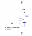
we were instructed to input parameters but there were some errors on my ltspice that i couldn't figure out how to fix it i have uploaded the parameters and the simulation i have done on lt spice
these are the results:

"Error on line 3 : m1 vout vin 0 n002 nmos l=0.25um lambda=0.06 gamma=0.4 kp=4e-3 vto=0.43v
Unknown parameter "lambda"
WARNING: Node VIN is floating.
WARNING: Node N002 is floating.
WARNING: Less than two connections to node VIN. This node is used by M1.
WARNING: Less than two connections to node N002. This node is used by M1.
WARNING: Less than two connections to node NC_01. This node is used by VDD.
Warning: Pd = 0 is less than W.
Warning: Ps = 0 is less than W.
Direct Newton iteration for .op point succeeded.
Semiconductor Device Operating Points:
--- BSIM3 MOSFETS ---
Name: m1
Model: nmos
Id: -1.91e-26
Vgs: 0.00e+00
Vds: -8.07e-17
Vbs: 6.52e-16
Vth: 4.66e-01
Vdsat: 3.72e-02
Gm: 5.96e-25
Gds: 2.43e-10
Gmb 1.95e-25
Cbd: 0.00e+00
Cbs: 0.00e+00
Cgsov: 1.40e-15
Cgdov: 1.40e-15
Cgbov: 1.82e-17
dQgdVgb: 5.15e-15
dQgdVdb: -1.40e-15
dQgdVsb: -1.40e-15
dQddVgb: -1.40e-15
dQddVdb: 1.40e-15
dQddVsb: 0.00e+00
dQbdVgb: -2.36e-15
dQbdVdb: 0.00e+00
dQbdVsb: 4.15e-30"
 

Attachments

WBahn

Joined Mar 31, 2012
30,071
What steps have you taken to try to fix it before posting it here?

**** Unknown parameter "lambda"

I think this may be a misleading artifact of the real problem. Look at your model definition. Why is it that you have the parameter 'l' in the model? Is it a legal parameter for the model?

Don't you think it might be a good idea to define a width for your transistor?

Have you taken the time to look at your schematic in light of the warnings you are being given?

**** WARNING: Node VIN is floating.

What is providing a signal to VIN?

**** WARNING: Node N002 is floating.

What node is N002? Check the netlist. You are also given a big hint below that it is used by M1. The connections for M1 are shown in the output you got:

**** m1 vout vin 0 n002 nmos

So N002 is the 4th pin, which is the bulk. You schematic would seem to indicate that this is connected to the source, which is the 3rd pin and which shows as being connected to node 0. So the netlist (which is what the simulator sees) says they are not connected. So look very closely at the schematic -- in particular, do you notice anything missing at the source that is present at the drain?

**** WARNING: Less than two connections to node VIN. This node is used by M1.

This is related to the first warning.

**** WARNING: Less than two connections to node N002. This node is used by M1.

This is related to the second warning.

**** WARNING: Less than two connections to node NC_01. This node is used by VDD.

Look at your schematic closely. Do you see any issues with the connections of the VDD supply?
 

Thread Starter

flyhigh09

Joined Apr 26, 2018
2
What steps have you taken to try to fix it before posting it here?

**** Unknown parameter "lambda"

I think this may be a misleading artifact of the real problem. Look at your model definition. Why is it that you have the parameter 'l' in the model? Is it a legal parameter for the model?

Don't you think it might be a good idea to define a width for your transistor?

Have you taken the time to look at your schematic in light of the warnings you are being given?

**** WARNING: Node VIN is floating.

What is providing a signal to VIN?

**** WARNING: Node N002 is floating.

What node is N002? Check the netlist. You are also given a big hint below that it is used by M1. The connections for M1 are shown in the output you got:

**** m1 vout vin 0 n002 nmos

So N002 is the 4th pin, which is the bulk. You schematic would seem to indicate that this is connected to the source, which is the 3rd pin and which shows as being connected to node 0. So the netlist (which is what the simulator sees) says they are not connected. So look very closely at the schematic -- in particular, do you notice anything missing at the source that is present at the drain?

**** WARNING: Less than two connections to node VIN. This node is used by M1.

This is related to the first warning.

**** WARNING: Less than two connections to node N002. This node is used by M1.

This is related to the second warning.

**** WARNING: Less than two connections to node NC_01. This node is used by VDD.

Look at your schematic closely. Do you see any issues with the connections of the VDD supply?
this was the given schematic, we were also tasked to find W which is really confusing for me. :/ and this is actually my first time using LTspice which was required to us, sry. :(
 

Attachments

WBahn

Joined Mar 31, 2012
30,071
I would then recommend that you go through some of the introductory tutorials available for LTSpice (of which there are probably thousands) in order to get a grasp on the fundamentals of simulation in general and LTSpice in particular.
 
Top