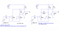
The original Q2 work in a common-base amplifier with current gain less then 1.
Additional transistor work as a CE amplifier. And CE amplifier has a large current gain.
So the small amount of current that open Q2 is enough to full open the Q3.
Excellent observation. I thought of adding the emitter follower, but didn't, for whatever reason. I have used that circuit as a zero crossing detector. See below.
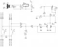
Thank you all very much, who helped me making a better circuit! I assembled it yesterday on the breadboard and it's working perfectly! However, i didn't completely understand the connection of those 3 transistors.The one in the original schematic was more clear to me.
Could someone help me understand it , please?
Whats the purpose of each transistor in the circuit(Q1, Q2, Q3)? i know that Q2 is connected common base mode,it has large voltage gain and no current gain ,Q3 emitter follower, etc ,but what what do they do assembled together?
In the original circuit whan i used FET anf those two transistors, PNP haven't been cut off completely with the inputs floating. How this problem is avoided in this circuit?
I would be very glad if someone explained more detail about those 3 transistors
This is the same schematic Ron H and Jony130 proposed, just redrawed by me to make a PCB.
Sensitive to what? I tried these values now, the delay is about 1 sec, i think a little longer is better.
I meant it's the same schematic considering transistors connection
Sensitive to what? I tried these values now, the delay is about 1 sec, i think a little longer is better.
I meant it's the same schematic considering transistors connection
By sensitive, I mean that the protection thresholds are slightly closer to zero volts with the 1Meg resistor, because the gains of the common emitter and common base circuits are both higher than with 47k.
47k and 470uF is almost exactly the same time constant as 1Meg and 2.2uF.
By sensitive, I mean that the protection thresholds are slightly closer to zero volts with the 1Meg resistor, because the gains of the common emitter and common base circuits are both higher than with 47k.
47k and 470uF is almost exactly the same time constant as 1Meg and 2.2uF.
I will use you recomended values then. Today I thought, that if some DC would be present in the inputs of the protection circuit, threre will be ~60V in case of a strong power amplifier, i thing the common base transistor would be burned-out then. Am i right?
 Facebook
 Google
 GitHub
 Linkedin
")