Long chain of MAX7219 Matrix displays Fail

Thread Starter

n4mwd

Joined Mar 21, 2016
50
Regarding the 0.1uF caps, I think I may go the 1206 route. All my stock here is 0805 so I'll have to order them. However, I could also use a wire to short across to the other trace and eliminate the extra copper.

The schottky diodes I mentioned before were SMT so I couldn't test with them easily. I did try with some axial lead 1N148's that I had laying around to make the diode clamps at the end like you said. They did seem to help a little with the unmodified control head. No change with the 4V modified head. But then gain, they aren't schottky.

One interesting fact is that with the modified control head, when I disconnected the logic analyzer from the end, the display went nuts and several modules failed very quickly. So if I disconnected the cable at the logic analyzer box, everything was fine. But when I disconnected it at the module, that's when it caused a problem. Its not connected to anything. Its just wires. Maybe some sort of stray capacitance?

I have some paper thin PCB blanks that I can make a board and glue it onto the back. As long as I don't use too much solder, I think it will fit. Tomorrow if I have time I will be designing a little buffer board and a diode clamp board.

One other thing is that I think my MAX chips are fakes. I got them off ebay (sold as real ones) and there have been many others say the same thing. If true, then the majority of commercial max modules out there are fake as well. Apparently, the fakes don't have the same 6V tolerance that the real ones have. However, I never would have bought the real MAX chips considering it would have cost $180 just for those chips alone. If I had it to do over, I would put a 50 cent busy bee 8051 on each module and drive the LEDs directly with that.
 

Sensacell

Joined Jun 19, 2012
3,787
It would be super helpful if you posted some pictures of the setup, this may help more than the 1000's of words.

A photo of the boards themselves.
A photo of the whole setup.
 

Thread Starter

n4mwd

Joined Mar 21, 2016
50
I took some photos this morning.

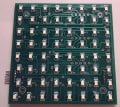
Here is the front size of the matrix without the bezel. Nothing special here. Just LEDs. These are 1206 because I needed to pass fat traces through the leads. Male connectors on the left, female on the right.
20180907_090638.jpg


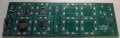
Here is a photo of the control head. There are four 7seg digits, a colon, and AM/PM indicator. The latter is probably hard to visualize, but its the group of LEDs on the upper right of the board. Power and USB connectors on the lower left. 3.3V linear reg on middle left. Control switches on upper left. Upper section of first digit contains the SiLabs UB3. The lower section of the first digit contains the buffer and a battery for the RTC. The upper second digit contains the RTC, crystal, and WifI module. The bottom of the 2nd digit contains the MAX7219 chip. The lower right of the board is the transistor that drives the AM/PM leds. It takes a PWM output from the CPU and drives the AM/PM leds through the resistors. Also in the lower right is a female connector for the first module.
20180907_090551.jpg

This is an example with the 11 modules. The first 9 are green and working properly, then a white one (#10), then a little commercial red one (#11) like in the photo I posted earlier. In this case, the logic analyzer probes are connected to the end of the chain, but not the actual analyzer. Its hard to tell here, but the "S" on #11 is deformed.
20180907_090100.jpg

This is the same as above, but with scrolling active. Normally the white module (#10) doesn't work, in this case it is. The red module (#11) is completely out at this point.
20180907_090148.jpg

Here is what happens when I disconnect the logic analyzer probes from the last module (Red #11). Notice that I've lost the "Y" and most of the time the comma too.
20180907_090226.jpg

Another photo with the probe wires disconnected. Module white #10 is flickering with garbage. Module #11 now has a deformed "S".
20180907_090242.jpg

Same thing.
20180907_090324.jpg
Here I have completely disconnected everything after module #9. The display is unstable starting at module #6.
20180907_090429.jpg

The probes add inductance and capacitance so removing them should make things better not worse. Could this be some sort of reflection?
 

Thread Starter

n4mwd

Joined Mar 21, 2016
50
I spent today designing, building, fabricating little buffer boards that use the same buffer that is on the control head. I soldered it on one of the matrices. The result was that the Display was much worse. Even the matrix with the buffer board failed.

I'll check it over again tomorrow to make sure I didn't goof up somehow, but this whole thing is getting ripe for the trash can really fast. The MAX 7219 is a very bad chip to design with.
 

takao21203

Joined Apr 28, 2012
3,702
You can try putting some small coils like 22uH

Some day I had a PIC32 powered from 5V through a red LED and it would reset quite easily when the board is touched, building a filter with some small coils, solved the problem.

I did build all myself and including long wires, the chip works at high frequency so they work like antenna, if touched, it draws enough power for a tiny moment the chip would reset.

think a LED has 30pF maybe but the noise is high frequency so propagates everywhere.

Electrolytics would do nothing, I tried of course.

But the problem was solved to full extent with some 2 small coils only..
 

Sensacell

Joined Jun 19, 2012
3,787
You can "buffer" the clock until you are blue in the face, but it wont help you here.

Re- read my rant in post #9 about GROUND.

This is a classic EE systems design problem, trying to clock circuits with fast SINGLE ENDED TTL pulses between multiple boards, all with HIGH CURRENT transients flowing in the ground is asking for trouble.

You can buffer away, but what the chip sees in it's remote corner of the universe is only the difference between it's LOCAL ground and the input.
This ground level can be all over the place, the poor chip sees a mess, even though it looks fine on the scope.

Differential signalling solves this problem by removing the local ground potential from the equation.
 

Thread Starter

n4mwd

Joined Mar 21, 2016
50
Can you post a schematic of your buffer board?
Its just the buffer chip with a 1N4148 feeding power to it. I will try to get it on the logic analyzer to maybe see what is going on. I have the actual schematic that I used to generate the board. I'll try to get it uploaded here along with a photo of how its attached to the board.

Differential signalling solves this problem by removing the local ground potential from the equation.
No argument, its just a matter of logistics. If I have to make too many mods to the module board then I might as well scrap it and go with a better design.

You can try putting some small coils like 22uH
The spikes have been 100nS pulses directly aligned with the CLK transitions. Despite the fact that a 6 foot signal line makes a really good antenna, there is nothing to say that this problem is caused by RFI. The logic analyzer shows no spikes outside of a communication burst. However, I might try a choke on the signal lines. The spike is 100nS and the half clock is 1000nS. The CS line is much greater.
 

Thread Starter

n4mwd

Joined Mar 21, 2016
50
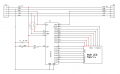
Here is the schematic of the buffer board and how it is attached to the board. Nothing special here.
BufferSchematic.png
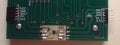
In this photo, J1 is on the right and the IC is mounted upside down to make the pcb route easier.
20180908_094955.jpg
 

Thread Starter

n4mwd

Joined Mar 21, 2016
50
I think these MAX chips must be possessed by silicon demons or something. I put the module with the buffer last in the chain. I hooked up the logic analyzer to the output. According to the logic analyzer, it was a near perfect pattern with virtually no spikes. Yet, nothing after the module with the buffer will work. Not even a little bit. If I put it first in the chain, nothing works.

The logic analyzer sees the same ground as the modules. I don't see why it would get a good signal and the modules get a bad one.

I also tried putting the signal lines at the end between two 1k resistors and vcc and gnd. Like this:
vcc ---/\/\/\/\-----signal--------/\/\/\/\-----GND
Didn't help.

What I am seeing, is that the spike occurs when there is a transition of some other signal line. So a LOAD transition can make a spike on the CLK line and a CLK transition can do the same on the LOAD line. I also occasionally see spikes on the data line. The data line comes from the previous module and not the control head.
 

ebp

Joined Feb 8, 2018
2,332
I don't see a decoupling cap on the board. If ever there was a part that needs good decoupling it is a clock driver. The decoupling must be on the driver side of the diode. Apart from probably poor signal shape, the diode and lack of decoupling will prevent the driver's output protection diode (output to Vdd) from being able to clamp any reflections.

Scratch the part about clamping. The datasheet is a bit cryptic, but it looks like the output may not have a diode to Vdd. There are words about partial power down (but not enough to explain anything, presumably in some ap info somewhere) and there is no spec for clamping current for output greater than Vdd.
 

ebp

Joined Feb 8, 2018
2,332
The buffer may well be responding to "spikes" of whatever origin and turning turning them from something the MAX would be unable to respond to into nice clean full-swing signals the MAX can. If the logic analyzer is asynchronous (which presumably it is, since there isn't anything to clock it other than the clocks themselves), it would have to sample at a rate comparable to the maximum allowable clock frequency for the MAX in order to have much hope of catching everything the MAX might.

What is odd in this (and maybe explained by details of the MAX operation) is that you never seem to get scrambled characters, as would be expected from bad clock signals. You just get blank modules - unless the photos just don't show scrambling.
 

Thread Starter

n4mwd

Joined Mar 21, 2016
50
I do get scrambled characters. Its just that they were feeling blank the day I photographed them. Sometimes, I get blinks which are supposed to be impossible. By that, I mean that the MAX chain is refreshed 4 times a second. So if it gets a scrambled message, it should stay that way until the next refresh in 1/4th second. In most cases, it does, but sometimes it just blinks on and off very rapidly.

I'm going to play around with adding caps like you said earlier and see if that helps. It may be necessary to use a larger case to fit them in. Beyond that, it looks like its scrap and redesign time. I might still use the MAX chips, but put a small 16 pin SOIC Busy Bee mcu with a half duplex differential transceiver on each module. That should prevent the MAX chip from spiking the signal bus and any misbehaving should be confined to that one module. According to the specs I read on the chip I like, the RS485 transceiver is supposed to be good enough for 256 modules and operate at 5Mbps.
 

ebp

Joined Feb 8, 2018
2,332
RS-485 transceivers are what I would use. There are many to choose from. If you need a lot on the bus then you must select those with fractional "unit load" (I can't remember how many "full load" are allowed). Many have "fail safe" inputs that give defined output state for various input fault conditions. Some of them are annoyingly expensive - more than lots of pretty decent microcontrollers.

Typically you would design the bus for reasonably constant impedance of about 100 ohms (I think 110 is what some of the really expensive cables are, but there is no compelling reason to use any specific impedance if cables aren't involved). Good impedance control on PCBs can be a bit of a challenge though it can be highly precise if done properly.

Usually you can get away without line termination if the bus isn't too long. Slew-rate limited drivers help with impedance issues and reflections, but of course they also limit the maximum clock rate.
 

Thread Starter

n4mwd

Joined Mar 21, 2016
50
While I was pondering the RS485 network it dawned on me that there wouldn't be any way to automatically serialize the modules. Right now, data shifts down the chain and each module gets its slice of the serial data stream. With a common bus RS-485, there is no way to do that. Each module would have to be custom programmed with a sequence number and no variation in physical order would be allowed. The modules would have to be serialized so they can be addressed properly.

I was thinking, that instead of an RS-485 bus, I could use a dual port I2C bus. That is, there would be two I2C ports on the MCU. One to communicate with the previous module and one to talk to the next module. That way, it would be trivial to serialize the units in the physical order they happen to be in. The I2C specs say it works up to 1 meter which is way more than I need to get to the next module.

Also, its bidirectional so it would be possible to error detect and correct packets due to the Busy Bee's built in 16-bit CRC. To send a message to the last module, it would have to be daisy chained down the line until it reaches its destination - error checked and corrected the whole way. Those MCU's are cheap and only cost about $13 for a pack of 25 (DigiKey). Using dual port I2C would eliminate the need for a separate RS-485 port.

The disadvantage is that I2C would have to be limited to about 100Kbps. However, since each Busy Bee has 8K of Flash I could put the character fonts in the MCU and then I need only specify each character by reference - not pixels. Also, since each module would have an mcu supervisor, there would be no need to constantly refresh the circuit. With the arrangement I have now, I have to send about 512 bytes to refresh the display and it has to be done 4x per second. With the Busy Bee's, I only need to send about 32 bytes every minute or when the display changes. So 100Kbps will be fine.
 

Thread Starter

n4mwd

Joined Mar 21, 2016
50
I went ahead and modded the boards to move the 0.1uF and 10uF caps closer to the MAX7219 chip. The idea is that this will help decouple power transients generated by the MAX.
20180910_111319.jpg
However, it actually seemed to make it worse. Here is the display with an 8MHz serial clock. Note again that the first modules are OK but later ones are bad. Its supposed to say "Monday". I have been experimenting with the clock speed. I tried 100 KHz, but it was much, much worse. At 1MHz, my usual speed, it wasn't really any different from 8MHz. I also had to use a longer LOAD pulse in order to get it this good.
20180910_111723.jpg

A source-end series damping resistor of something in the 10 to 50 ohm range might be tolerable on the data and clock lines.
Been thinking about this one. What about putting a 10-50 ohm resistor on every module in series with the CLK and LOAD line at the chip? My rationale is this . The display line is configured as one giant shift register. There is only one LOAD pulse. So when LOAD goes high, ALL of the modules simultaneously load the data. So all of them are doing the same thing at exactly the same time. The theory is that a series resistor from the bus to the MAX chip will limit the ability of the MAX chip to mess with the bus signal.

Does this sound like it might work? If so, what value resistor would be best?

In the mean time, I will work on the schematic for the MCU supervised module discussed above and will post it when its done.
 

Thread Starter

n4mwd

Joined Mar 21, 2016
50
Here is the schematic I came up with for an MCU controlled version. This way, each MAX chip has its own controller on the module. The EFM8BB1 Busy Bee is a 16 pin SOIC MCU. It will read I2C from the input side, error check and correct the packet, then retransmit it to the next module in the chain. Meanwhile, display data that is addressed to this module is sent to the MAX chip via SPI MOSI. The data out from the max chip is routed to SPI MISO. The Busy Bee is 3.3V logic which is why there is a 3.3V regulator and a lot of resistors. MCU outputs to the MAX are Open Collector with 5V pullups. MAX data out goes through a voltage divider to the MISO port.

In theory, shifting zeros into the MAX chip, without changing LOAD, should give the bits that were in the MAX shift register. This would detect a false clock pulse which would skew the data, but would not be able to tell if a false LOAD pulse caused skewed data to get loaded into the internal MAX registers.
MatrixMCU.png
I'm going to try the resistor in series with the LOAD and CLK lines on each module first, but given that nothing else has worked, I went ahead and drew the schematic for the MCU controlled version. I was thinking that 1K series resistors would be a better value. 100 ohms seems too small.
 

Thread Starter

n4mwd

Joined Mar 21, 2016
50
I think I am finally on to a real solution. I went ahead and cut the traces and soldered 2K resistors inline with the CLK and LOAD lines. The placement of the module that has the little buffer board doesn't seem to matter now. Here is the revised schematic. The new resistors are in the red circle. This seems the most solid design change of all. So far, not a single error after running for over an hour. The Logic analyzer is not attached either. Its solid enough that I will go ahead and make some more modules now.
Matrix-fixed.PNG
 

Thread Starter

n4mwd

Joined Mar 21, 2016
50
OK, that was the solution. I modified the PCB's to have 2K resistors inline with the LOAD and CLK lines from the bus as per the schematic above. The result is that the display instantly became totally stable. Since I already made one module into a buffer module, I placed it about halfway. Testing showed no errors in several hours.

The total length of the matrix chain is about 6 feet. If I had to do this again, I would go with something like RS-485 or a daisy chained I2C bus. However, this proves that it can be done with 18 jumbo matrix modules out to 6 feet.

20180915_134506.jpg
 

ebp

Joined Feb 8, 2018
2,332
Without scoping the signals it is hard to say just what the resistors are doing.

Part of the effect is to introduce a low-pass filter formed by the IC's input capacitance and the resistor. That's often a bad thing to do, but the chip has hysteresis on those inputs so it will tolerate slow transitions with no problem and the clock rate isn't very high. The filter will work from "both sides" of the resistor - if there is noise on the clock it will filter some of that, if the the IC ground bounces (as it will), it will defend the clock input from some of that. The blasted datasheet doesn't have a spec for input capacitance.

The resistors may also be serving to damp reflections on the lines. When you've just got inductance and capacitance, energy just keeps getting shuttled back and forth between. The resistors would dissipate some energy.

The resistors would also limit current into input protection diodes, such as may exist, due to clock line transients beyond the supply rails.
 
Top