Long chain of MAX7219 Matrix displays Fail

Thread Starter

n4mwd

Joined Mar 21, 2016
50
I am building a rather large clock from 8x8 matrix displays using the MAX7219 connected in series. If I have 4 or less modules connected, it seems to work fine. More than 4 and there is an obvious problem as the farther modules don't seem to be working properly.

The MAX7219 is basically a shift register. Data is shifted into the first module which shifts into the second and so forth until it gets to the last module. Each MAX chip has a Data In and Data Out pin. Each 8x8 matrix is 4"x4" square. So the length of the data line is only about 4" to the next module. The Clock and LOAD lines run the length of the entire display (6 feet) and are buffered from the CPU using a 74LVC2G17W6-7 which is a 2 input high current output non-inverting buffer.

I did a static DC test on the CLK and LOAD lines from the buffer and they do not show any significant signal drop all the way out to 10 modules. HOWEVER, when I hooked up the logic analyzer, it is showing 100 nS transient noise at regular intervals. The yellow circles are the spikes that are creeping into the circuit. When the spike occurs on the SS(LOAD) line, it causes the shift register in the MAX chip to load prematurely which makes the MAX chip freak out and display strange stuff.

There have been several people post across the net about this same problem, but I haven't found anyone with a solution yet. I have noticed that the length of the SS/LOAD pulse seems to make a difference. The max7219 is not a true SPI chip so it isn't supposed to require the SS/LOAD line to go low before the data starts, however, it seems to work better when I do it that way. I made it go low just before the end of the data and high just after and it made it worse.

Using a 0.1uf capacitor across the LOAD and GND will help in certain circumstances. I have to slow the clock rate down to 1 MHz or else it makes it worse. When I slowed it all the way down to 100 KHz, there was no difference to 1 MHz.

The spikes (circled in yellow) are present whether I have 10 modules or zero. However, the first modules in the chain don't seem to care about them for unknown reasons.

Anybody know what is going on here?

The buffer 74LVC2G17W6-7 is a schmidt trigger rated at 125 MHz and 32 mA which may mean that it might be overly sensitive to noise. Would a slower buffer be a better choice?

Is there some way to filter out the 100 nS spikes?

Thanks.


cap1.GIF


cap2.GIF

cap3.GIF
 

Thread Starter

n4mwd

Joined Mar 21, 2016
50
Note that the CPU I am using is a Silicon Labs EFM8UB3 which is a 48 MHz 8051. I control the timing of the CS/SS/LOAD line, but the CPU drives the the CLK and DATA lines automatically. The transient spikes are 100 nS wide and tend to occur in groups of 1,2, 3 or 4. They are most common on the CS/SS/LOAD line, but can also be seen occasionally on the CLK and DATA lines as well.

Would buffering the CS/SS/LOAD and CLK lines on every module help?

Note that I tried a 1K termination resistor to ground on the CS/SS/LOAD line at the end of the chain and it only helped slightly. It also got hot so it was pulling some current.
 

dendad

Joined Feb 20, 2016
4,476
Is this running on 5V?
What sort of resistor is the 1K? I'm surprised a 1K resistor gets hot on 5V, unless it is a very low power rated one.
Check your power supply volts I reckon.
 

nsaspook

Joined Aug 27, 2009
13,272
Show us your wiring diagram for individual chip power and bypassing. This is when you need a good DSO to see the actual waveform.
 
Last edited:

hexreader

Joined Apr 16, 2011
581
Can't help but wonder....

Might re-writing the code in MCU cure the problem?

Instead of filtering out the spikes, fix the MCU/code to prevent them being generated in the first place. Perhaps use shadow registers to write a whole port at a time rather than messing with individual IO bits?

Just guessing, since we have little information to go on, but it does sound like that sort of a problem to me. Could be wrong.
 

Thread Starter

n4mwd

Joined Mar 21, 2016
50
Thanks for the replies. Sorry it took me so long to reply. Been out today.

Is this running on 5V?
What sort of resistor is the 1K? I'm surprised a 1K resistor gets hot on 5V, unless it is a very low power rated one.
Check your power supply volts I reckon.
It runs on a 4 Amp 5V wall wort switching power supply. The actual voltage is between 4.8V and 5.25V. Not as solid as I would like, but still within specs. The CPU is a SiLabs EFM8UB3 8051 which runs on 3.3V supplied through a little dedicated linear regulator. The SPI outputs from the CPU are buffered and stepped up to 5V using the 74LVC2G17W6-7 buffer. The max chips are all 5V, but will accept 3.3V logic. So the first one in the chain gets a 3.3V logic DATA IN. DATA OUT from the first MAX chip is then 5V logic.

Show us your wiring diagram for individual chip power and bypassing. This is when you need a good DSO to see the actual waveform.
Or a good analog logic analyzer - which I don't have either. I will try to get a schematic and upload it tomorrow. Each MAX7219 is powered with 5V from the system control board or previous Max module. Each has its own 0.1uF and 10.0 uF bypass capacitors as required by the MAX 7219 spec.

Might re-writing the code in MCU cure the problem?
Instead of filtering out the spikes, fix the MCU/code to prevent them being generated in the first place. Perhaps use shadow registers to write a whole port at a time rather than messing with individual IO bits?
I don't use a library for the SPI, I just use the onboard SPI peripheral which handles SPI generation. I have checked it thoroughly and there is nothing in the firmware that is directly responsible for the spikes. The spikes are only 100 nS wide so if it was the firmware, it would have to be something like "SPI_CS = HIGH; SPI_CS = LOW;" as each instruction takes about 21 nS to execute. With the exception of the spikes of unknown origin, the logic analyzer says that the firmware is generating the proper logic patterns.

As a test, I moved, in firmware but not hardware, the SPI_CS line to another pin. The Line was free of spikes. This would imply that they spikes are from the MAX7219 chips.

NEW THEORY

I haven't had a chance to test this yet, but I noticed before by accident that the MAX7219 array will still work even without VCC power. It obviously draws current from the clock and data lines and shouldn't. The max LED arrays normally get VCC power from the previous max array. So each MAX array draws current, and because the 4" PCB trace with the 5V is essentially a low ohm resistor, each module is powered with successively less voltage than the previous module. The difference between the first and last module should be measurable.

The 5V control lines, CLK/LOAD, are powered by that 5V high power buffer chip. Those lines also go through the same amount of PCB copper, but because they are only used as inputs, the current draw is much less which means that the voltage at the end of the chain will be higher than the VCC voltage. I suspect that this is what is causing the spikes on the control lines because if the chip has the ability to backfeed power in from the control lines, and since they aren't shorted, they must be interconnected though semiconductor material acting like a diode. So when the control lines are LESS voltage than VCC, it shouldn't backfeed.

I will test this tomorrow and report back.

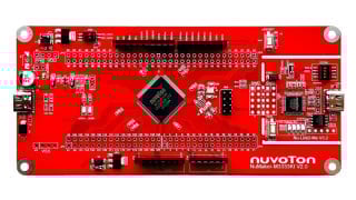
The following is a picture of a commercial version of the MAX7219 matrix module that I found online. Mine is the same schematic (except they don't have C2), but with a much larger LED matrix. I will try to get some real pictures and schematics uploaded tomorrow.
 

Thread Starter

n4mwd

Joined Mar 21, 2016
50
...Perhaps use shadow registers to write a whole port at a time rather than messing with individual IO bits?...
This would not be easy to do on the SciLabs EFM8UB3 due to the use of a priority crossbar. Honestly, I have never tried it. The crossbar routes each pin into a particular internal peripheral that the programmer selects, but I honestly don't know what would happen if I tried to read or write a pin or port that has been assigned to a peripheral through the crossbar. Normally when I need a direct port I/O pin, like I do for the CS line, I have to mark the pin as SKIPPED by the crossbar.

So my guess is that doing a read-modify-write on a full port that has crossbar assignments could mess things up.
 

Thread Starter

n4mwd

Joined Mar 21, 2016
50
What sort of resistor is the 1K? I'm surprised a 1K resistor gets hot on 5V, unless it is a very low power rated one.
It was just a 1/4W axial lead resistor I had laying around that I shoved into the output connector of the last matrix module. It wasn't hot enough to burn, but it was very noticeably warm - like very warm bath water. Since the 5V buffer is a push-pull type, the pull-up resistor turned out to be a bad idea. Nevertheless, it did help a little which would support my new theory - see above.
 

Sensacell

Joined Jun 19, 2012
3,447
"If I have 4 or less modules connected, it seems to work fine."

This would be the tip off for me.

Trying to run fast digital signals over janky long wires with a ground that carries large currents is a ticket to hell.

The logic signals here are ground referred, the signals are only as good as the ground they are referenced to.
You have large and fast current transients flowing in the ground, this creates voltage drops that will corrupt the logic signals.

You need to bypass the supply voltage with capacitors all along the chain, with both large electrolytics and smaller ceramic capacitors.
Beef up the size of the ground conductor, keep it short as possible.

Large LED displays typically use differential signalling to combat this problem, making ground noise less of an issue.
 

Thread Starter

n4mwd

Joined Mar 21, 2016
50
As promised, here is the schematic and photos...

This is the controller which has a built in MAX7219 chip. Most of the actual schematic has been deleted for simplicity.
controller.png
Here is the individual matrix schematic. Note that it is designed to be daisy chained.
Matrix.png
Here is a photo of the actual matrix module - front view with an 8 pin DIP for size reference.
Matrix-Front.jpg
 
Last edited:

Thread Starter

n4mwd

Joined Mar 21, 2016
50
UPDATE

To test my theory (above), I disconnected the matrix chain from the controller board and then reconnected the Data, Vcc and Gnd with wire jumpers. Then I connected the CLK and CS lines directly to the CPU pins which are 3.3V logic. According to the logic analyzer, there were significantly fewer spikes and only on the CS line, but unfortunately, they were still there.

So my theory seems to be on the right track. I'm thinking about cutting some traces and power the buffers with 3.3V instead of 5V. I think the CPU can only push 12mA so it might not be enough to make it all the way down the chain.

Another thing I might try is to set the CPU pins to be open collector and then use a resistor pullup at the end of the chain. That way the 5V MAX chips are all getting 5V logic but the control lines are guaranteed not to exceed Vcc.
 

Thread Starter

n4mwd

Joined Mar 21, 2016
50
The logic signals here are ground referred, the signals are only as good as the ground they are referenced to.
You have large and fast current transients flowing in the ground, this creates voltage drops that will corrupt the logic signals.

You need to bypass the supply voltage with capacitors all along the chain, with both large electrolytics and smaller ceramic capacitors.
Beef up the size of the ground conductor, keep it short as possible.

Large LED displays typically use differential signalling to combat this problem, making ground noise less of an issue.
Each MAX chip has a 0.1 uF and a 10 uF cap between VCC and Gnd. I tried connecting a long ground wire directly from the controller to the end of the chain, but that made it worse. The same when I connected the VCC that way. I then connected a 1000 uF electrolytic between the Vcc and Gnd at the end of the chain. I think it made a slight improvement, but not very significant.

On the controller board, the Vcc and Gnd PCB traces are 5mm wide. On the Matrices, the traces are 2.5mm wide. They take the shortest route possible straight across the board.
 

Thread Starter

n4mwd

Joined Mar 21, 2016
50
I'm thinking about grouping these into 3 modules and using either a separate buffer or an RS232 driver to segregate the data lines from the others. Does this sound like it will work? The buffer solution would be a lot easier and cheaper. The using RS232 level signal lines would probably make it less sensitive to noise.
 

Sensacell

Joined Jun 19, 2012
3,447
Use differential signalling - a pair of differential line drivers and line receivers.
It's extra wires, but this will make it fast and bulletproof.

RS-232 hardware is too slow and cumbersome.
 

Thread Starter

n4mwd

Joined Mar 21, 2016
50
Use differential signalling - a pair of differential line drivers and line receivers.
It's extra wires, but this will make it fast and bulletproof.

RS-232 hardware is too slow and cumbersome.
Differential would work. It would be the best way to communicate. I'm in the middle of two protocols. The finished display is 6 feet long which is a little too long for TTL and a little too short for differential. I found a UA9637 differential receiver chip that is under $2 that might do the job. The specs don't explicitly mention a speed, but judging from the propagation delays, it should be able to handle 5 Mbps easily. I am working at 1 Mbps.

If I understand you correctly, you are talking about using a two RS485 drivers (CLK and LOAD) (4 wires) at the control head, and then receivers on a common bus every third module. This would certainly work as long as fan out isn't an issue.

It's safe to say I won't be using the MAX7219 chip for future designs so its a matter of salvaging this project more than making it bulletproof. The spikes are definitely coming from the MAX7219 chips and not RFI. Even with differential signalling, there is absolutely no practical way to validate that the MAX7219 chip received the data correctly. I could shift out what's in the chip and check that, but to do that, I have to shift something else in - which could have errors.

With RS232 level signalling, I meant that each module triplet would have an pair of receivers and a pair of transmitters to daisy chain the CLK and LOAD signals down the chain. So the longest path would be about 1 foot. The advantage over differential is that no extra wires are required.

The next time I ever do this, I will use a small mcu for every module and drive the LED's directly. This would have the advantage of making the module smart and giving it the ability to error detect and correct. If I use RS485 for the signalling, only a single pair of wires is necessary because I could make a network out of it.
 

ebp

Joined Feb 8, 2018
2,332
I would try adding an electrolytic capacitor of 100 µF or so to each board's supply. From the photos it appears that the caps used for decoupling are both ceramic. The excellent high-frequency performance of ceramic caps can actually sometimes result in resonance with the power distribution inductance and make things worse instead of better. The arrangement of more or less parallel tracks for power and ground will create quite substantial inductance (putting them "on top" of each other on opposite sides of the PCB is better). A bulk capacitor on each board will not only improve decoupling for the high currents of the LEDs but push the resonant frequency down and add some high-frequency loss (cap equivalent series resistance) that can help damp resonance.

You might improve matters a bit by terminating the far end of the clock lines with resistors to bias the line at 2.5 volts (i.e. 2 equal resistors, one to gnd one to Vcc). Since you aren't using a line driver or a proper transmission line, there is likely little point in aiming for anything like what you would use for those (term at characteristic impedance). I'd try something in the range of about 2k for each resistor. This of course increases the loading on the driver, but the drivers you are using can source and sink over 30 mA with 5 V supply. Biasing the line at the centre of the swing keeps the loading of the source and sink drivers about equal. If ringing is a problem, sometimes clamping the far end of the line with Schottky diodes to supply and ground can help. If you mount them on a plug so they can plug in in place of another board, add a good decoupling cap along with the resistors and/or diodes.

The inputs of the MAX chip are not compatible with 3.3 V signals. The specified minimum HIGH level is 3.5 V.
 

Thread Starter

n4mwd

Joined Mar 21, 2016
50
If ringing is a problem, sometimes clamping the far end of the line with Schottky diodes to supply and ground can help.
I'm not sure I understand. You mean reverse biased diodes across the power lines?

I may have made an error on the PCB design in that C1 and C2 are too far from the chip. What do you think?

Regarding VIL on the the MAX chip, you are correct and I missed that. Most 5V chips go down to 2V, but not this one. However, in the current design, only the DATA IN on the first chip gets that logic level which seems to work OK and the rest go through the buffer. Subsequent data lines are driven by the previous 5V chip in the chain. This does explain why bypassing the buffer to drive the CLK and LOAD lines with 3.3V does not work.

I have convinced myself that a big part of the problem is that modules farther down the line are getting lower Vcc voltage due to resistance. However the driver has less load so it can exceed Vcc. In my experiments bypassing the LOAD buffer and using and open collector on the MCU, and a pull up resistor at the end of the chain were successful. The pull up resistor at the end of the chain ensures that the LOAD line never exceeds the last module's Vcc. Using Open collectors on the CLK line did not work. I suspect 1MHz was too fast for it given the capacitance of the line.

As such, I'm thinking that cutting the Vcc trace of the buffer and soldering in a forward biased diode to reduce the logic driver voltage to around 4.3V. This would handle CLK and LOAD at the same time.

Previously, I did try a 1000uF cap at the end of the line and it did help, but only modestly. The caps on the board now are 10uF and 0.1uF. I can't go much higher than 10uF chip ceramic due to size restrictions. However, another 10uF closer to the max chip would be doable. There is no room on the front side of the board because that is where the LED matrix is located. The cover comes down in between them and anywhere else would alter the light patterns. The control board has some room on the front, but not the modules.

I'll play around with some extra caps and see if it helps.
 

ebp

Joined Feb 8, 2018
2,332
The diodes are for clamping the signal lines, so two diodes in series, cathode of one to Vcc, its anode and the cathode of other to signal, anode of second to ground. These will clamp signal excursions beyond the supply rails. The "best" choice is usually signal type Schottky diodes. The purpose is two-fold - it limits the voltage that can be applied to an input and it "eats" energy that would otherwise reflect back and make ringing of the unterminated line worse.

From the absolute max specs of the MAX IC, it appears that the serial-related inputs are tolerant of 6 V regardless of the IC's supply voltage (note difference in way the specs for different pins are written). This could be verified by very carefully raising the voltage of (say) a clock input of an un-powered IC while monitoring the current. I'd use a 10k resistor in series, just for safety (and as a "shunt" for measuring the current). If you can get to 6 V with no current or only low microampere current into the input, it confirms the interpretation of the specs. Maybe something in the text of the datasheet discusses this. Note the limit of voltage below ground.

A very large cap at the far end is likely to be much less effective than distributed bulk caps. I would use radial leaded types soldered to one or the other of the boards' connectors if space permits. Suitable caps should be no more than about 6.5 mm in diameter.

C1 is probably close enough. C2 is too far away to effectively decouple the MAX, but is typical of where a "bulk" capacitor would normally be. If Maxim recommends 10 µF for the IC itself, it should be closer. With small surface mount caps there isn't a lot to be gained by using a low value in parallel with a high value. That was true with leaded parts where the higher value part would have more parasitic inductance. If you doubt the decoupling of the MAX, I'd suggest increasing the value of C1. Stay away from Y5V or Z5U or similar types. They have horrendous negative voltage coefficient of capacitance and can be down to 20% of nominal capacitance if run at near their rated voltage. X5R or X7R are far from perfect in this regard but are much better.

Normally I'd recommend a tightly twisted pair of perhaps 20 AWG to route supply and ground to the far end of the board string, but this is rather in conflict with the single-ended signal problem. It might be worth a try. Single wires will have a lot of inductance and again, with ceramic-only decoupling could make for very large transients due to resonance. Some decent bulk capacitance is necessary in such a case.

A source-end series damping resistor of something in the 10 to 50 ohm range might be tolerable on the data and clock lines.

It is really very difficult to diagnose what is required without an oscilloscope.
 

Thread Starter

n4mwd

Joined Mar 21, 2016
50
I finally got enough time to try something. There have been a lot of good suggestions here and I thank all of you for them, but since this is a one-off design, I have to start with the simplest, not necessarily the best idea.

What I did was to cut the VCC trace to the buffer and solder in a 1n4148 smt diode which drops the supply voltage to the buffer to about 4V. I wanted to use a diode that has a lower forward voltage, but that is what I had on hand. I did have a schottky, but its VF was too low at 200mV. Anyhow, doing this limits the max Voh to just under the buffers supply voltage which should be about 4V. This is above the minimum VIH requirement of the MAX chip.

The result was that the first nine modules (3 lineal feet) operated nearly flawlessly. It took about 30 minutes for the first one to fail. However, modules 10 and 11 failed almost instantaneously. In previous tests, all modules started failing simultaneously within a few seconds. I am speculating that now there is a new problem - the signal lines are running out of juice before they get to the end.

The diodes are for clamping the signal lines, so two diodes in series, cathode of one to Vcc, its anode and the cathode of other to signal, anode of second to ground. These will clamp signal excursions beyond the supply rails. The "best" choice is usually signal type Schottky diodes. The purpose is two-fold - it limits the voltage that can be applied to an input and it "eats" energy that would otherwise reflect back and make ringing of the unterminated line worse.
I didn't understand what you meant before, but now I do. This is definitely something to put on the last module to clamp the voltages. Like I mentioned before, I have some 200 mV schottkys that should work nicely. I have a second, unmodified control head that I can try this with.

Regarding the location of C1, the issue is not the physical distance to the chip, but the length of the traces. When I designed the PCB, I was trying to use larger traces and avoid using vias. The reason is that I made about 3 or 4 failed boards by hand and soldering vias is a real pain. The Vcc line actually makes a long loop to get around a via and then back up to C1. The Vcc line is simply too fat to fit between an 0805 cap. When making ones own boards by hand, fatter traces are easier to deal with.

The 0.1uF is a X7R and the 10uF is a X5R. I will try to mod the boards and get the caps closer in. I'll probably just leave the existing 10uF where its at and add a new one next to C1. I wish there was enough room for an electrolytic, but there isn't.

I already tried running power to the end of the line with wires. Made it worse. I did use a pullup resistor at the end before. I said before that it was a 1K, but that was my error. I misread the color bars and it was actually 100 ohms. The point is that it was getting very warm at the end of the chain. That was going through the buffer and not when I was bypassing with an open collector driver from the mcu. I used real 1K pullups for the open collector testing and they did not get warm.

The logic analyzer works fairly well, but it has no analog inputs. An oscilloscope or a logic analyzer with analog inputs would answer a few questions.

In the firmware, I can increase the refresh rate and insert code to reset each MAX chip with each refresh. So a failure every 30 minutes is acceptable to me since the next refresh cycle will clear the error. Without the mod, the display was too messed up and no amount of refreshing would fix it.

I'm thinking the next step is to group the modules into three's, add a buffer with a 1n4148 and diode clamps at the end. That should carry me out to module 18.
 

ebp

Joined Feb 8, 2018
2,332
Yes, you're quite right about the decoupling. I didn't look carefully and failed to notice that long loop which certainly will impair decoupling. The inductance may be sufficient to cause some nasty ringing. If you scraped off some solder mask you might be able to use a 1206 part from the existing ground connection to the Vcc track going to the IC pin. A through-hole part could be used.

So there isn't clearance to use a radial electrolytic laid flat on the solder side of the board and soldered to the pins of the I/O connector? I can find 47 µF 6.3 V that are 5 mm OD. There is no need to derate voltage for aluminum caps. Alternatively, you could add some more 10 µF ceramics quite easily if you scraped some solder mask off the Vcc and ground tracks. Even adding two more, one against the pins of each connector, might help. You can probably find 1206 that are sufficiently low profile at 22 µF and probably higher at 6.3 or 10 V.

I don't understand why you want to reduce the amplitude of the clocks. As I mentioned before, it certainly appears that there is no issue with the clocks going to 6 V abs max regardless of the MAX supply voltage. The resistance of the clock lines will be trivial in terms of attenuation at the far end. The resistance of the ground lines is more likely to cause grief due to LED current. You could do some assessment of the latter by only lighting up one or two LEDs per module. Adding ground jumper wires from input to output connector of each module would reduce the resistive loss but do virtually nothing to reduce inductance.

You might try using a low-value series resistor at the clock driver output. I'd be inclined to try something around 15 to 20 ohms. It will slightly reduce the clock slew ratel. The hysteresis at the MAX inputs will cope with low slew rate, but differences between thresholds from one chip to another could be detrimental in terms of violation of data setup and/or hold times if the slew rate were too low.

It would help somewhat with damping reflections that return to the source. Again, it is all just guesswork without an oscilloscope.
 
Top