LED2001PHR DC-DC buck converter problem

Thread Starter

MrCooI

Joined Sep 10, 2019
5
Hello!

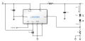
So I wanted to design a driver for my laser diodes and flashlight LEDs up to 4A. I found this "LED2001PHR" ic and it seemed very convincing until I tried it out. I copied the circuit from ST EdesignSuite (https://www.st.com/content/st_com/en/support/resources/edesign.html):
d1fa7bf0727016ea104398c672fbefb4 (1).png
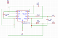
I created my PCB using EasyEDA because it is easy-to-use and offers free shipping on the first order. Here is my schematic:
d1fa7bf0727016ea104398c672fbefb4 (1).png
And I created a PCB design using this schematic:
d1fa7bf0727016ea104398c672fbefb4 (1).png
And the bottom layer:
d1fa7bf0727016ea104398c672fbefb4 (1).png
My main goals are small size (10*15mm) and the 4A maximum output current.

I can set the output current with the R_S resistor (Iout = 100mV/R_S). I tried to make the ground lines as thick as possible to minimize the trace resistance around the sense resistor (by my calculations it is around 3.5mΩ). I ordered every possible combination of inductors and capacitors to be able to build the most efficient circuit for every LEDs from 1A to 4A. If I put a 30mΩ resistor, the resulting resistance considering the PCB trace resistance is ~33.5, and the output is 3A. I tried 4 other R_S values and I always got the correct Iout by using the 100mV/(R_S+3.5mΩ) formula.

So basically it works great until I cross 3A. If I put a 22, 25, 27mΩ sense resistor the whole thing stopped working. I use my adjustable power supply to test the circuit, with the 30mΩ resistor, the current consumption was 1-1.1A on 15V (I used a 5V, 3A diode) and if I put the 27 or 25mΩ resistor and set the current limit to 4.3A, the consumption is 4.3A on 6.5V (5V 4A diode). I tried to set the current limit to 5A, then the whole thing burned. First I thought that the Chinese supplier sent some trash sense resistors, so I ordered 22, 25 and 27mΩ resistors from a local store and the results were the same. I also considered that they accidentally sent me LED2000 ICs (similar to LED2001 with 3A maximum output current), but the label clearly says LED2k1.

I destroyed 10 ICs now, so I have no idea what to do.

So, my question is: does anybody know what am I missing here?

Thanks in advance
 

Attachments

MisterBill2

Joined Jan 23, 2018
18,176
Two things apparent: Your layout shows pin 9 grounded, the reference circuit does not show it connected. AND it may be that you are exceeding the safe operating area of the device in a manner that does not trigger the self protection function. That has the possibility of leading to overheating and destruction. Maximum ratings are not just suggestions, they are real limits.
 

Thread Starter

MrCooI

Joined Sep 10, 2019
5
Two things apparent: Your layout shows pin 9 grounded, the reference circuit does not show it connected. AND it may be that you are exceeding the safe operating area of the device in a manner that does not trigger the self protection function. That has the possibility of leading to overheating and destruction. Maximum ratings are not just suggestions, they are real limits.
Well, I'm pretty sure I'm not exceeding the safe operating area of the device since the datasheet and all ST pages say 4A. My driver stops working if the current consumption is bigger than 3A. The output current should be around 4A using the 22mΩ resistor. Pin 9 is not present in the reference circuit, that's true. The datasheet says: "Exposed pad - Connect the exposed pad to AGND "
 

Delta Prime

Joined Nov 15, 2019
1,311
This may be obvious but ... May I ask. Which package style are you using in your design? The pin assignments for VFQNPN "Vs" SO8-BW are different.
 

Delta Prime

Joined Nov 15, 2019
1,311
If you're using the ST EdesignSuite you can simulate your LEDs, lasers, in fact all the values for support circuitry components . You no longer have to blow up components. equation
Rs =100mV/4A=25mΩ. Take a look at
Component selection
6.8.1 Sensing resistor
In closed loop operation of the LED2001 datasheet.
 

Thread Starter

MrCooI

Joined Sep 10, 2019
5
If you're using the ST EdesignSuite you can simulate your LEDs, lasers, in fact all the values for support circuitry components . You no longer have to blow up components. equation
Rs =100mV/4A=25mΩ. Take a look at
Component selection
6.8.1 Sensing resistor
In closed loop operation of the LED2001 datasheet.
I'm sorry, but I don't get your point here. I used that formula to calculate the value of the resistor, and the IC doesn't work for me if the sense resistor is below 30mΩ. If I put a 25mΩ and switch off the current limit, then it burns and I don't know why.
 

Alec_t

Joined Sep 17, 2013
14,280
The board layout shown in the datasheet has a large ground plane on the bottom layer, with thermal vias going to the pad under the IC. Your layout offers less heatsinking for the IC. The ratings specified are for the IC mounted on the dev board (which presumably is similar to the datasheet board), so perhaps with reduced heatsinking you shouldn't expect 4A capability. Even so, it's surprising the IC fails, given that it has inbuilt thermal protection.
 

Delta Prime

Joined Nov 15, 2019
1,311
In your design circuit there is no load .there is no LEDs.buck regulator can be seen that the output voltage appearing across the load is sensed by the sense / error amplifier and an error voltage is generated that controls the switch. When the switch in the buck regulator is on, the voltage that appears across the inductor is Vin - Vout
The LED manufacturer typically provides the equivalent dynamic resistance of the LED biased at different DC currents. This parameter is required
(Rsense÷Number of leds × dynamic resistance of leds + Rsense). Just as you calculated the trace resistance in added to Rsense.
 
It looks to me like you have a layout problem. I think you are sensing current across a length of trace / ground plane and Rs. This wouldn't be as much of a problem at much lower currents, but the resistance of the added trace is probably a large portion of the 25 or 30 milli Ohms you are trying to sense across. I also suspect a similar problem on the ground side of Rs.

SenseLines.png

The data sheet shows them separated on their schematic.
DataSheet.png
This suggests to me that pins 9, 4, and the low side sense of Rs should be outside of the high current path.
 

MisterBill2

Joined Jan 23, 2018
18,176
It looks to me like you have a layout problem. I think you are sensing current across a length of trace / ground plane and Rs. This wouldn't be as much of a problem at much lower currents, but the resistance of the added trace is probably a large portion of the 25 or 30 milli Ohms you are trying to sense across. I also suspect a similar problem on the ground side of Rs.

View attachment 198930

The data sheet shows them separated on their schematic.
View attachment 198929
This suggests to me that pins 9, 4, and the low side sense of Rs should be outside of the high current path.
A higher sense resistance would result in a lower current output, and in addition, the failure happens when the current sense resistor value is TOO LOW. So while the flaw you describe is real it is not likely to cause an overload failure.
I suggest checking for signs of instability at the higher loads, that is leading to destruction.
 

TeeKay6

Joined Apr 20, 2019
573
Two things apparent: Your layout shows pin 9 grounded, the reference circuit does not show it connected. AND it may be that you are exceeding the safe operating area of the device in a manner that does not trigger the self protection function. That has the possibility of leading to overheating and destruction. Maximum ratings are not just suggestions, they are real limits.
The schematic does not show pin9 grounded, but the text(sec 2.2) of the datasheet instructs that it should be connected to ground. It is not obvious how the T.S. made the connection as the pad is not accessible outside the outline of the part. Perhaps the T.S. can tell us how he managed to solder the pad of the IC to the pad of the PCB.
 

MisterBill2

Joined Jan 23, 2018
18,176
I had not considered the soldering to the copper under the IC at all, but certainly those maximum specifications are achieved with optimum heat sinking, which often is described in some detail, including a statement of the thermal resistance. In every case, device capabilities with no heat sinking will be less.
 
I have had problems with this kind of package not soldering well on the pad under the package. It can be difficult to know it's soldered when soldering by hand.

Do you have a way of monitoring the temperature of the IC? A thermocouple or an IR thermometer might tell a lot.
I wonder if it is somehow lingering between the 125C upper spec and the 150C thermal shutoff.
 

MisterBill2

Joined Jan 23, 2018
18,176
One option may be to create a THIN copper heat sink that would fit under the IC, and be soldered to it. That heat sink could then extend out the ends and have a radiating area. Yes, the copper will indeed need to be fairly thin, not over 0.020 inch, and very flat. Soldering would have to be done per the specified process, what ever is described in the application notes.
At the very least it will be very wise to read everything the maker says about heat sinking and under what conditions that higher current rating is applicable.
 
Top