LED FLASHING RATE CONTROL USING PIC16F684

Thread Starter

Don Omar

Joined May 5, 2017
49
I need help with programming the pic16f684 using assembly
i need to program it to control the led flashing rate which is connect it to pic RC5
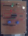
i manage to find the code to flash the led and i tried it on my circuit and its working fine
the only thing now i need is the code to control the flashing rate using potentiometer wish is connect it to pin RA1
Code:
LIST P=PIC16F684
include P16f684.inc

__CONFIG _CP_OFF & _WDT_OFF & _BOD_OFF & _PWRTE_OFF & _INTRC_OSC_NOCLKOUT & _CPD_OFF

org 0x00
reset
goto start
org 0x04
start bcf STATUS, RP0             ;Bank 0
bcf STATUS, RP1
clrf PORTC                            ;Clear PORTC
bsf STATUS, RP0
clrf TRISC                          ;PORTC is OUTPUT
bcf STATUS, RP0
loop
bsf PORTC,0X05                      ;Set RC5 HIGH
call delay
bcf PORTC,0X05                      ;Set RC5 LOW
call delay
goto loop
;————————————
delay
movlw 0xFF
movwf 0x51
CONT1 movlw 0xFF
movwf 0x52
CONT2 decfsz 0x52,f
goto CONT2
decfsz 0x51,f
goto CONT1
return
;————————————
end
Mod edit: code tags
 

Dodgydave

Joined Jun 22, 2012
11,395
Download datasheet, look at page 68, there is a working example, note the A/D result is put into two files as it's a 10bit converter.
ADRESL
ADRESH

You can determine which lower 8bits is put into ADRESL (right justified less accurate ) or Upper 8bits (left justified more accurate) is put into ADRESH by selecting Left or Right Justified. You then look at those files for your result.

https://www.google.co.uk/url?sa=t&s...ggzMAI&usg=AFQjCNGsXfZvv2eIpdVAe8kVCz3LMF5rcQ
 
Last edited:

Thread Starter

Don Omar

Joined May 5, 2017
49
Download datasheet, look at page 68, there is a working example, note the A/D result is put into two files as it's a 10bit converter.
ADRESL
ADRESH

You can determine which lower 8bits is put into ADRESL (right justified less accurate ) or Upper 8bits (left justified more accurate) is put into ADRESH by selecting Left or Right Justified. You then look at those files for your result.

https://www.google.co.uk/url?sa=t&s...ggzMAI&usg=AFQjCNGsXfZvv2eIpdVAe8kVCz3LMF5rcQ
 

Thread Starter

Don Omar

Joined May 5, 2017
49
Dodgydave thanks for replaying
Could you please help me write the code
Because I have no clue what I'm doing
Thanks
 

Dodgydave

Joined Jun 22, 2012
11,395
Copy the example in the datasheet on pg68, i would select Left justified, then the result of the AD will be in ADRESH, you then use this value to put into your file.

here is one i did for a 16F690 for a variable delay on port AN0,
Code:
;************************************************************************
  AD               ; A/D ROUTINE

    MOVLW b'00000001' ;Left justified, Vdd Vref, AN0 source input
    MOVWF ADCON0      ; A2D routine  conversion
    BSF ADCON0,GO     ;Start conversion
    BTFSC ADCON0,GO  ;Is conversion done?
    GOTO $-1         ;No, test again
    MOVFW ADRESH     ;Read upper 8 bits
    MOVWF RESULTHI
    BSF STATUS,RP0   ;Bank 1
    MOVFW ADRESL     ;Read lower 2 bits
    BCF STATUS,RP0   ;Bank 0
    movwf RESULTLO   ; save result lo
    return

Delay
    call AD              ; get values
    incfsz    RESULTLO,f   ; incriment file to zero (inc instead of dec to reverse pot direction)
    goto $-1             ; repeat
    incfsz RESULTHI,f    ;increment file to zero
    goto $-3
    return
Mod edit: code tags
***************************************************************


NOTE I USED BOTH ADRESH AND ADRESL to make my delay by moving them into temporary files RESULTHI, RESULTLO
 
Last edited by a moderator:

LesJones

Joined Jan 8, 2017
4,511
Here is an example of using the ADC on a PIC16F88. The code should be very similar for the PIC that you are using. The code is for a four channel sequencer. Each ADC input controls the time of each step of the sequence.

Code:
;Sequencer
;
;28/06/16
; Version 01 now being modified for 4 channels (Renamed to Sequencer_02.asm)
;


; I/O port useage

;   RA0   (Pin 17)   Analog in 0
;   RA1   (Pin 18)   Analog in 1
;   RA2   (Pin 1)     Analog in 2
;   RA3   (Pin 2)     Analog in 3
;   RA4   (Pin 3)
;   RA5   (Pin 4)     Vpp for programming
;   RA6   (Pin 15)  
;   RA7   (Pin 16)  

;   RB0   (Pin 6)     Channel 0 out
;   RB1   (Pin 7)     Channel 1 out
;   RB2   (Pin 8)     Channel 2 out
;   RB3   (Pin 9)     Channel 3 out
;   RB4   (Pin 10)
;   RB5   (Pin 11)
;   RB6   (Pin 12)   PGC for programming
;   RB7   (Pin 13)   PGD for programming


   list P=16F88
   #include p16f88.inc

;Program Configuration Register 1
     __CONFIG  _CONFIG1, _CP_OFF & _CCP1_RB3 & _DEBUG_OFF & _WRT_PROTECT_OFF & _CPD_OFF & _LVP_OFF & _BODEN_OFF & _MCLR_OFF & _PWRTE_ON & _WDT_OFF  & _INTRC_IO

;Program Configuration Register 2
     __CONFIG  _CONFIG2, _IESO_OFF & _FCMEN_OFF

; Define variables at memory locations

;*******************************************************************************
; Constants
;*******************************************************************************


RAM_START  equ  0x20


; The periods are timed with timer1 which is set to run at the internal clock
; rate (4 Mhz) of Fosc/4 or 1.0MHz which is equal to a 1 uS period.


;*******************************************************************************
; File Register Variables
;*******************************************************************************
  cblock  RAM_START

Save_STATUS     ;Save during interrupt
Save_W       ;Save during interrupt
Save_PCLATH     ;Save during interrupt
Save_FSR     ;Save during interrupt  

param1:   1  ; parameter 1  (Used in delay cycles routine)
param2:   1  ; parameter 2  (Used in delay cycles routine)

AD_Delay:   1   ;Delay count to allow AD to sample input

CH_Time:   1

AD_Channel:   1   ;AD channel number

  endc


; start at memory 0

   org   0
   goto   SETUP
   org   4
   goto   INTERRUPT


Init:
SETUP:
   clrf   PORTB     ; port B outputs low
   clrf   PORTA     ; port A output low
   bsf     STATUS,RP0   ; select memory bank 1

; set inputs/outputs
   movlw   B'00000111'   ; comparators off
   movwf   CMCON
   movlw   B'11110000'   ; port B 0 to 3 outputs 4 to 7 inputs
   movwf   TRISB     ; port B data direction register
   movlw   B'00111111'   ; outputs (0) and inputs (1)
   movwf   TRISA     ; port A data direction register
   movlw   B'11000000'   ; settings (pullups disabled TMR0/2)
   movwf   OPTION_REG

; analog inputs, A/D 

   movlw   B'00001111'   ; AN0 to AN3 are analog inputs
   movwf   ANSEL     ;Bank 1
   movlw   B'01000000'   ; left justified A/D result, VCC as ref
   movwf   ADCON1     ;Bank 1

   bcf     STATUS,RP0   ; select memory bank 0
   movlw   B'01000000'   ; Fosc  1/8 for  4MHz system clock 
   movwf   ADCON0     ; Bank 0
   bsf     ADCON0,ADON   ; A/D on
   bsf     STATUS,RP0   ; select memory bank 1
   movlw   B'01101000'   ;  for 4 MHz
   movwf   OSCCON     ; Bank 1


; Initialized Timer 1
   bcf     STATUS,RP0   ; select memory bank 0
   MOVLW   B'00110100'   ;Clock source FOSC, 1:8 prescale, Dedicated Timer1 oscillator circuit disabled,
  ;Do not synchronize external clock input, Fosc/4 Timer off
         ;So counter will increment every 8 uS  (4 Mhz clock)
         ; So for overflow after 500 ms (62500 * 8uS ) counter would need to be loaded with 0x0BDC

   MOVWF   T1CON     ;With 4 Mhz clock timer will increment every 500 mS


START:

Main_Loop:

Time_CH0:
   BSF   PORTB,0     ;1 cycle  (Set channel 0 output)
   MOVLW   0x00     ;Select channel 0
   MOVWF   AD_Channel  
   CALL   Read_Analog
   CALL   Channel_Delay
   BCF   PORTB,0     ;1 cycle  (Clear channel 0 output)


Time_CH1:
   BSF   PORTB,1     ;1 cycle  (Set channel 1 output)
   MOVLW   0x01     ;Select channel 1
   MOVWF   AD_Channel  
   CALL   Read_Analog
   CALL   Channel_Delay
   BCF   PORTB,1     ;1 cycle  (Clear channel 1 output)


Time_CH2:
   BSF   PORTB,2     ;1 cycle  (Set channel 2 output)
   MOVLW   0x02     ;Select channel 2
   MOVWF   AD_Channel  
   CALL   Read_Analog
   CALL   Channel_Delay
   BCF   PORTB,2     ;1 cycle  (Clear channel 2 output)


Time_CH3:
   BSF   PORTB,3     ;1 cycle  (Set channel 1 output)
   MOVLW   0x03     ;Select channel 3
   MOVWF   AD_Channel  
   CALL   Read_Analog
   CALL   Channel_Delay
   BCF   PORTB,3     ;1 cycle  (Clear channel 1 output)

   GOTO   Main_Loop


;     -----------------------------------------------------

; Interupt handler  (Interrupts not used.)

INTERRUPT:
;Save various registers

   MOVWF Save_W     ;Save W  
   MOVF STATUS, W  
   CLRF STATUS      ;Bank 0 will be selected
   MOVWF   Save_STATUS
   MOVF   PCLATH, W
   MOVWF   Save_PCLATH
   MOVF   FSR, W
   MOVWF   Save_FSR


;Restore registers

   MOVF   Save_FSR, W
   MOVWF   FSR
   MOVF   Save_PCLATH, W
   MOVWF   PCLATH  
   MOVF   Save_STATUS, W  
   MOVWF    STATUS  ;Restore STATUS  
   SWAPF    Save_W, F  
   SWAPF    Save_W, W  ;Restore W  
   RETFIE

;     -----------------------------------------------------
;Subroutines

Read_Analog:       ;Channel number will be in AD_Channel (Bits 0 - 2)
         ;Result returned in "W"

   RLF   AD_Channel   ;Move bits to required position (Bits 5 -3)   ;1 cycle
   RLF   AD_Channel   ;1 cycle
   RLF   AD_Channel   ;1 cycle
   BCF   ADCON0, 3   ;1 cycle
   BCF   ADCON0, 4   ;1 cycle
   BCF   ADCON0, 5   ;1 cycle
   MOVF   AD_Channel, W   ;1 cycle
   IORWF   ADCON0, F   ;Select channel   ;1 cycle

   MOVLW   D'40'     ;1 cycle       64 decimal
   MOVWF   AD_Delay   ; acquisition time  1 cycle

Dec_AD_delay:             ;loop is 3 cycles long (64 x 3 = 192
   DECFSZ   AD_Delay,f   ;1 cycle  (2 on exit)
   GOTO   Dec_AD_delay   ;2 cycles
   BSF     ADCON0,2     ; GO/DONE bit start conversion
WAIT_AD_Ready:
   BTFSC   ADCON0,2     ; conversion complete when cleared ~11 cycles
   GOTO   WAIT_AD_Ready
   MOVF   ADRESH,w
   RETURN     ;2 cycles


Channel_Delay:
   MOVWF   CH_Time   ;1 cycle
   INCF   CH_Time   ;So that AD value of zero does not give maximum time

CH_Loop:
   DECFSZ   CH_Time   ;1 cycle (2 cycles on exit)
   GOTO   CH_Delay
   GOTO   CH_End

CH_Delay:     ;This generates one unit of channel delay
;   CALL   DELAY_100mS   ;100mS * 256 =25.6 seconds
;   CALL   DELAY_50mS   ;50mS * 256 =12.8 seconds
   CALL   DELAY_20mS   ;20mS * 256 = 5.12 seconds

   GOTO   CH_Loop

CH_End:
   RETURN     ;2 cycles


Delay:

DELAY_100mS:
; Value for param = (100000 - 14)/8 = 99986/8 = 12498 = 0x30D2

   MOVLW   0x30     ;   (1 uS)    (1 cycle)
   MOVWF   param2     ;   (1 uS)    (1 cycle)
   MOVLW   0xD2     ;   (1 uS)    (1 cycle)
   MOVWF   param1     ;   (1 uS)    (1 cycle)
   GOTO   delay_cycles

DELAY_50mS:
; Value for param = (50000 - 14)/8 = 49986/8 = 6248 = 0x1868

   MOVLW   0x18     ;   (1 uS)    (1 cycle)
   MOVWF   param2     ;   (1 uS)    (1 cycle)
   MOVLW   0x68     ;   (1 uS)    (1 cycle)
   MOVWF   param1     ;   (1 uS)    (1 cycle)
   GOTO   delay_cycles     ;Not needed as delay_cycles follows on from here.

DELAY_20mS:
; Value for param = (20000 - 14)/8 = 19986/8 = 2498 = 0x09C2

   MOVLW   0x09     ;   (1 uS)    (1 cycle)
   MOVWF   param2     ;   (1 uS)    (1 cycle)
   MOVLW   0xC2     ;   (1 uS)    (1 cycle)
   MOVWF   param1     ;   (1 uS)    (1 cycle)
;   GOTO   delay_cycles     ;Not needed as delay_cycles follows on from here.

;*******************************************************************************
; Function:  delay_cycles
; Description: Delay a specified number of instruction cycles including
;  interrupt cycles.  The function call overhead adds between
;  13 and 16 cycles of delay on top of the specified value.
; With 4 Mhz system clock and 1:8 prescale
;Delay will be  param * 2 uS + (13 * 1uS)  + 0 to 3 uS
;     = param * 8 uS + (13 to16.0 uS)  (Use 14 uS for calculation.)
;  So param = No. of (uS-14)/8
; Parameters:  param1 - least significant byte of 16 bit cycle delay
;  param2 - most significant byte of 16 bit cycle delay
; Returns:  None
;*******************************************************************************
delay_cycles:
  comf  param1,F  ; negate the delay by complementing the     (1 uS)    (1 cycle)
  comf  param2,F  ; low and high bytes         (1 uS)    (1 cycle)
  bcf  T1CON,TMR1ON  ; stop timer 1           (1 uS)    (1 cycle)
  movf  param1,W  ; move the low byte of the delay into     (1 uS)    (1 cycle)
  movwf  TMR1L  ; timer 1           (1 uS)    (1 cycle)
  movf  param2,W  ; move the high byte of the delay into     (1 uS)    (1 cycle)
  movwf  TMR1H  ; timer 1           (1 uS)    (1 cycle)
  bcf  PIR1,TMR1IF  ; clear the timer 1 rollover flag     (1 uS)    (1 cycle)
  bsf  T1CON,TMR1ON  ; turn on timer 1         (1 uS)    (1 cycle)
  
tmr1_check:  
  btfss  PIR1,TMR1IF  ; wait for the timer 1 rollover flag to     1 uS while looping    (2 uS) (2 cycle) on exit
  goto  tmr1_check  ; trigger
  return         ;             (2 uS)   (2 cycle)


   END
The interupt handler code is not used so you can ignore it.

Les.
 
Last edited by a moderator:

Thread Starter

Don Omar

Joined May 5, 2017
49
Copy the example in the datasheet on pg68, i would select Left justified, then the result of the AD will be in ADRESH, you then use this value to put into your file.

here is one i did for a 16F690 for a variable delay on port AN0,

;************************************************************************
AD ; A/D ROUTINE

MOVLW b'00000001' ;Left justified, Vdd Vref, AN0 source input
MOVWF ADCON0 ; A2D routine conversion
BSF ADCON0,GO ;Start conversion
BTFSC ADCON0,GO ;Is conversion done?
GOTO $-1 ;No, test again
MOVFW ADRESH ;Read upper 8 bits
MOVWF RESULTHI
BSF STATUS,RP0 ;Bank 1
MOVFW ADRESL ;Read lower 2 bits
BCF STATUS,RP0 ;Bank 0
movwf RESULTLO ; save result lo


return


Delay
call AD ; get values
incfsz RESULTLO,f ; incriment file to zero (inc instead of dec to reverse pot direction)
goto $-1 ; repeat
incfsz RESULTHI,f ;increment file to zero
goto $-3
return
***************************************************************


NOTE I USED BOTH ADRESH AND ADRESL to make my delay by moving them into temporary files RESULTHI, RESULTLO

hey dodgydave
please mate help me with the whole code from start to end
because i have no clue what to do
i tried to use the one you send me and i did not manage to go further
im still strangling
 

nerdegutta

Joined Dec 15, 2009
2,689
hey dodgydave
please mate help me with the whole code from start to end
because i have no clue what to do
i tried to use the one you send me and i did not manage to go further
im still strangling
Hi.

Is this homework or a school project?

No one here will write the code for you, but we will point you in the right direction, and tell you which datasheets to read and guide you when you are stuck.

You have to read the datasheets, show us your code, and tell us exactly what you have done. Including schematics/ picture of breadboards.
 

djsfantasi

Joined Apr 11, 2010
9,237
I tried but it did not work
So that's why I asked for the whole code so I can copy it and paste
Thanks
Are you reading the posts from those trying to help you?

Is this homework or a school projecct?

No one here will write the code for you...

You have to read the datasheets, show us your code, and tell us exactly what you have done. Including schematics/ picture of breadboards.
 

Dodgydave

Joined Jun 22, 2012
11,395
Use YOUR SET up, then Call up My AD routine in Post#7, with the results in Resulthi, Resultlo, and set your led on to your desired port bit, use My delay in Post#7, and then clr the led off, call my delay, put led on and repeat...
 

Thread Starter

Don Omar

Joined May 5, 2017
49
hey dear,
to answer your question yes its a university work has to be ready in one week.
as you can see from the photo there is 2 potentiometer one to control the brightness and one to control the flashing rate
the one with the green wire attached to it is the one am using at the moment
i manage to find one for the led brightness control its working fine ,i do not know how to create another one to control flashing rate and combined both of the them in one code.
this is the code i have so far :
Code:
TITLE "pwm_led.asm" ;
List P=PIC16F684, R=DEC
INCLUDE "p16f684.inc"

; data segment
CBLOCK 0x20
del ; variable used for delay
temp ; local temp variable
ENDC

; code segment
PAGE
__CONFIG _FCMEN_OFF & _IESO_OFF & _BOD_OFF & _CPD_OFF &
_CP_OFF & _MCLRE_OFF & _PWRTE_ON & _WDT_OFF & _INTRC_OSC_NOCLKOUT
org 0 ; start program at the beginning of mem
bcf STATUS, RP0 ; activate BANK 0
clrf PORTA ; initialize PORT A
clrf PORTC ; initialize PORT C
movlw 0x07
movwf CMCON0 ; comparators OFF
bsf STATUS, RP0 ; change to BANK 1

; ADC and PWM configuration
bsf TRISA ^ 0x80, 0 ; enable input on pin A0
bsf ANSEL ^ 0x80, 0 ; configure A0 as analog input
movlw b'01110000' ; set ADC Frc clock
movwf ADCON1 ^ 0x80
movlw 0xFF
movwf PR2 ^ 0x80 ; PWM period 244Hz
bcf TRISC ^ 0x80, 5 ; enable RC5 for output
bcf STATUS, RP0 ; back to BANK 0

bsf ADCON0, 0 ; Left justify, Vdd Vref, AN0, On
movlw 7
movwf T2CON ; enable Timer 2 with 1:16 prescaler
movlw 0x0C ; enable single output PWM
movwf CCP1CON

loop
movlw 20
movwf del
call delay ; 20 msec delay

bsf ADCON0, GO ; start ADC operation
btfsc ADCON0, GO ; and wait for its completion
goto $-1

bsf STATUS, RP0 ; change to BANK 1
movf ADRESL ^ 0x80, w ; read 2 lower bits of ADC
bcf STATUS, RP0
movwf temp
rrf temp, f
rrf temp, f
movf temp, w
iorlw b'11001111'
andwf CCP1CON, f ; setup the 2 lower bits of PWM
movf ADRESH, w ; get high 8 bits of ADC
movwf CCPR1L ; setup PWM duty cycle

goto loop ; endless loop


; procedures
delay ; a delay for del milliseconds
movlw 200

sublw 1 ; this loop takes 5us*200 = 1ms
sublw 0 ; for PIC16F684 @ 4 MHz
btfss STATUS, Z
goto $-3

decfsz del, f
goto delay
return

end
Mod edit: code tags
 

Attachments

Last edited by a moderator:

absf

Joined Dec 29, 2010
1,968
In your first post you said
i need is the code to control the flashing rate using poteniameter wish is connect it to pin RA1
But in your code it is
Code:
; ADC and PWM configuration
bsf TRISA ^ 0x80, 0 ; enable input on pin A0
bsf ANSEL ^ 0x80, 0 ; configure A0 as analog input
Which ADC input are you using?

pic16f684.jpg
Which LED are you trying to lite on RC5?

Allen
 

Thread Starter

Don Omar

Joined May 5, 2017
49
In your first post you said


But in your code it is
Code:
; ADC and PWM configuration
bsf TRISA ^ 0x80, 0 ; enable input on pin A0
bsf ANSEL ^ 0x80, 0 ; configure A0 as analog input
Which ADC input are you using?

View attachment 126232
Which LED are you trying to lite on RC5?

Allen
hey ALLEN,
trying to lite the white led and i manage to get it to work using input AN0
the thing now how can i CONTROL USING AN1?
dont worry about the red and green leds
 
Top