LED DC-DC boost converter output gets too hot after modification.

Thread Starter

Tank Circuit

Joined Mar 5, 2017
31
Essentially my question is why a150v FDD770N15A Mosfet gets too hot when the 100v NCE0110K Mosfet stays cool?
In my attempts to better understand how to drive MOSFETs with PWM signals I have decided to make a bench lamp from an LED TV backlight I pulled from a TV with a cracked screen. Since all the LEDs are in series it needs a voltage between 90VDC (dim) and 96VDC (bright). I purchased two cheap driver/boost CV LED circuits from eBay (https://www.ebay.com/itm/10-42-Inch...h=item1ee6971e0b:g:p90AAOSwP79bWEhi:rk:1:pf:0). It bumps the 12VDc up to 87VDC and it runs forever without any thermal runaway. Since this is only enough voltage for a night light, I decided to see what I can do to up the voltage output.
I determined a slight reduction of the resistance of R4 in the voltage divider would increase the output voltage. I place a 100k potentiometer across the resistor and carefully changed the value while monitoring the output voltage. I determined that changing the value of R4 from 510R to 470R would bring the output voltage to 97VDC. Before I committed to this modification I performed a long test. I thought It was working great until I started to notice a hot smell as it flickered and died.
I soon discovered that the maximum voltage of the original Mosfet is 100VDC, I figured it shorted because the voltage was too close to the maximum limit to be in a safe operating range. Upon further investigations, I saw that the Schottky diodes and the output filter capacitor also have the same 100v limit.
So I decided to increase the voltage limits and try again. A new capacitor and Schottky (a single 150VDC 5A) was easy, but finding a new Mosfet is another story. I searched and I found what I assumed was a perfect upgrade, the 150v FDD770N15A Mosfet.
Original 100V: http://www.hytic.net/upload/files/2017/09/NCEPOWER-NCE0110K.pdf
Replacement 150V: http://www.mouser.com/ds/2/149/FDD770N15A-483941.pdf

While I waited for this new Mosfet to arrive I did some testing with the other undamaged board and I discovered that I can modify R4 slightly and can bring the output voltage to 94VDC without any thermal runaway. The output stays under 50c after hours of running (without any heatsink applied). I would go with this configuration except that I'm too close to the upper limits of the Mosfet. I am ready for the new part to make this a rugged design.

I finally get the new parts, and It works great until the voltage goes above 92.5VDC (not quite bright enough for my eyes). going above this level causes it to start to get hotter and then the characteristics must change and the voltage will start creeping up causing more heat, etc. etc. etc. I even added a heatsink but it still can reach over 100c.

What is different between the datasheets making the weaker Mosfet perform at higher voltages?

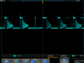
The input PWM gate voltage is 12VDC at 100khz-400khz (it is currently running at 119khz). The controller is a BIT3260 from BiTEK wired in a Constant Voltage (CV) configuration. All the factory schematics show it with the CC design. If you use those and this sloppy schematic you should understand how it works.
https://pdf-datasheet-datasheet.netdna-ssl.com/pdf-down/B/I/T/BIT3260-BeyondInnovationTechnology.pdf
https://manualzz.com/doc/17445444/1

Obviously, I have selected the wrong replacement Mosfet, can someone help me decide on a better alternative?
 

Attachments

Sensacell

Joined Jun 19, 2012
3,784
The heating is probably due to insufficient gate drive.

The replacement has a lower RDSon than the original, it should run cooler.
This indicates that it's probably not switching fully ON, or is doing it slower.

1) The replacement has double the gate charge.
(more current is needed to charge and discharge the gate capacitance in the same time period)
2) The replacement has double the max gate threshold voltage.

Have you checked the gate signal with an oscilloscope?
 

ArakelTheDragon

Joined Nov 18, 2016
1,366
In other words, the cooling for the old one is not good for the new one. More than 1W can not be dissipated without a cooler system, the old cooling system is set for the old transistor.

Options:
1. Suggested by "Sensacell" - check how the transistor works.
2. Get a better cooling system.

I suggest you listen to "Sensacell", you will understand more about MOS FET transistors.
 

Audioguru

Joined Dec 20, 2007
11,248
The original has the low threshold voltage as a logic-level Mosfet and the replacement needs much more gate voltage to turn on the same amount.
 

Thread Starter

Tank Circuit

Joined Mar 5, 2017
31
Thanks for everyone the feedback. I do agree that the heat is because the internal resistance is too high. I suspected there would be a difference since the original was an "Enhanced Mode Power Mosfet" and the replacement is called a "Power Trench Mosfet".

Which brings me to this query: when I was in school we learned about FETs, now there are a gamut of options. Not saying I have a problem with the different types since they all have an important function in today's electronics, but it seams as if each manufacturer has coined their own label, such as:
Trench Power (Fairchild)
"OptiMOS-3" Power-Transistor (Infineon)
Enhancement Mode and
Enhancement Mode Power MOSFET (NCE)
Large-signal Power MOSFET (Sanyo)
to name a few that I found today.
where does it end, and is there going to be any structure to the names?

Sensacell stated:
1) The replacement has double the gate charge.
(more current is needed to charge and discharge the gate capacitance in the same time period)
2) The replacement has double the max gate threshold voltage.

Have you checked the gate signal with an oscilloscope?

Do you think I could modify the gate resistors (perhaps I can remove them both) to allow this replacement to work, or should I opt for a new replacement? Any suggestions?
I have checked the gate waveform and I am getting the full 12 VDC rail voltage.

The input allows for 12-24VDC but the IC's VCC is limited by the 14 volt zener. I am running this from a 12V source.
 

ebp

Joined Feb 8, 2018
2,332
Measure the actual supply voltage of the IC. The IC datasheet is useless, but if the IC supply is at least 10 V or so there should be no problem driving the replacement FET adequately assuming the chip maker isn't grossly incompetent in making the output drive circuit. The threshold of the replacement FET is a bit higher, but the total gate charge is considerably lower. It isn't impossible, but I seriously doubt gate drive problems unless the supply voltage to the IC is sagging.

Currents. Look at currents. Everybody always wants to look at voltages and ignores currents. Because the load is a string of LEDs the output current is very sensitive to the output voltage. A small increasing output voltage can result in a significant increase in output current - which is why the LEDs get brighter. This means higher input current not only because the output current is higher but because the duty cycle must increase. It may be pushing the inductor closer to saturation, which means even higher peak current in the switch. Switch instantaneous conduction loss when ON is proportional to the square of the current. There is no cycle-by-cycle current limiting for the FET.

Don't forget that getting the heat out of the FET relies on it being properly soldered to the foil. If the foil was damaged in any way in removing the original part or the soldering of the drain to the foil is not well done in the replacement, heat transfer could be significantly compromised.
 

crutschow

Joined Mar 14, 2008
38,503
it seams as if each manufacturer has coined their own label, such as:
Trench Power (Fairchild)
"OptiMOS-3" Power-Transistor (Infineon)
Enhancement Mode and
Enhancement Mode Power MOSFET (NCE)
Large-signal Power MOSFET (Sanyo)
to name a few that I found today.
where does it end, and is there going to be any structure to the names?
Except for the phase "Enhancement Mode" all those labels are mainly advertising jargon and have no useful meaning to the designer using them.
There is no end, of course, to such jargon. :rolleyes:
 

ArakelTheDragon

Joined Nov 18, 2016
1,366
Except for the phase "Enhancement Mode" all those labels are mainly advertising jargon and have no useful meaning to the designer using them.
There is no end, of course, to such jargon. :rolleyes:
Which is a very bad practice and it causes problems for hardware developers as they are stupid(this is what we are called) and they can not develop hardware.........

Thanks for everyone the feedback. I do agree that the heat is because the internal resistance is too high. I suspected there would be a difference since the original was an "Enhanced Mode Power Mosfet" and the replacement is called a "Power Trench Mosfet".

Which brings me to this query: when I was in school we learned about FETs, now there are a gamut of options. Not saying I have a problem with the different types since they all have an important function in today's electronics, but it seams as if each manufacturer has coined their own label, such as:
Trench Power (Fairchild)
"OptiMOS-3" Power-Transistor (Infineon)
Enhancement Mode and
Enhancement Mode Power MOSFET (NCE)
Large-signal Power MOSFET (Sanyo)
to name a few that I found today.
where does it end, and is there going to be any structure to the names?

Sensacell stated:
1) The replacement has double the gate charge.
(more current is needed to charge and discharge the gate capacitance in the same time period)
2) The replacement has double the max gate threshold voltage.

Have you checked the gate signal with an oscilloscope?

Do you think I could modify the gate resistors (perhaps I can remove them both) to allow this replacement to work, or should I opt for a new replacement? Any suggestions?
I have checked the gate waveform and I am getting the full 12 VDC rail voltage.

The input allows for 12-24VDC but the IC's VCC is limited by the 14 volt zener. I am running this from a 12V source.
If it is the resistors I am thinking about, they are pull-up and pull-down resistors, do not remove them no matter what!
 

Thread Starter

Tank Circuit

Joined Mar 5, 2017
31
Thanks, everyone. I have a different Enhanced Mode Mosfet on order that might work better.
https://www.mouser.com/datasheet/2/427/91300-61907.pdf
IRL540

I agree that the problem has to do with the gate voltage.
I went back a looked at the gate waveforms on both the working and on with the replacement (gets too hot) Mosfet. They both are identical with a PWM signal measuring 12V p-p, but they had very different Drain waveforms.
I see on the working device there is a bit of ringing noise right after the pulse is applied followed by the decaying sinuous ringing from the large inductor.
On the unit with the replacement Mosfet, there isn't the noisy ringing after the PWM pulse, it's nice and clean, but I see the decaying pulses from the coil are not present after all of these ON/OFF periods. It appears the Mosfet isn't ON hard enough to trigger the coil to start its discharge cycles. It seems to miss a couple or three ON/OFF sessions before it is actually activated (It looks like it might be active for a couple of cycles before it goes inactive again). It seems to scroll through the pluses. So the Mosfet is doing too much work and the coil is on vacation for most of the time and it appears to me that heat is the byproduct.

I opted for another 100V max Mosfet since finding one above that rating with the same gate and amperage specs proved to be very difficult.
I drew a rough sketch of the waveforms (those are supposed to be perfect sinuous shapes).Waveform of hot MOSFET.png
 

ebp

Joined Feb 8, 2018
2,332
"I agree that the problem has to do with the gate voltage."
I don't agree.

"I went back a looked at the gate waveforms on both the working and on with the replacement (gets too hot) Mosfet. They both are identical with a PWM signal measuring 12V p-p ..."

12 volts is plenty of drive for either FET.

Can you add some voltages to the waveform sketches? It looks like you did the sketches with a mouse. If you can, it would probably be better to draw them on paper and photograph or scan the drawing. It is quite important to know what parts of the waveform are flat-topped/bottomed, what parts have more rounded tops & bottoms, and comparative rise and fall times - which make the transitions very quickly and which are slower. I'm trying to get an idea of whether some of that is actually spurious switching or actual ringing. The fact that the part after what appears to be the first clean pulse is shown with both a "top" and "bottom" on the same part suggests an oscilloscope triggering issue or perhaps that two differing pulse types are being produced and superimposed. Are you using an analog or digital scope? If digital, single-shot triggering may help resolve this.
 

ArakelTheDragon

Joined Nov 18, 2016
1,366
"I agree that the problem has to do with the gate voltage."
I don't agree.

"I went back a looked at the gate waveforms on both the working and on with the replacement (gets too hot) Mosfet. They both are identical with a PWM signal measuring 12V p-p ..."

12 volts is plenty of drive for either FET.

Can you add some voltages to the waveform sketches? It looks like you did the sketches with a mouse. If you can, it would probably be better to draw them on paper and photograph or scan the drawing. It is quite important to know what parts of the waveform are flat-topped/bottomed, what parts have more rounded tops & bottoms, and comparative rise and fall times - which make the transitions very quickly and which are slower. I'm trying to get an idea of whether some of that is actually spurious switching or actual ringing. The fact that the part after what appears to be the first clean pulse is shown with both a "top" and "bottom" on the same part suggests an oscilloscope triggering issue or perhaps that two differing pulse types are being produced and superimposed. Are you using an analog or digital scope? If digital, single-shot triggering may help resolve this.
Take a picture of the osciloscope or screenshot.

I don't get this: PWM, MOS, but you want a sin signal on the gate?
 

Thread Starter

Tank Circuit

Joined Mar 5, 2017
31
The problem was the PWM controller IC the whole time.

My old analog scope here at home makes troubleshooting very hard.
So I took these boards to work. What a difference a 1ghz MSO Tektronix makes (see the waveforms attached).
Here are the good board waveforms: Gate and drain.
Good Gate.png good output.png

I soon realized that the bad board has a burst of output pulses (at 110khz) followed by a long inactive period (these bursts were at a 12.5khz rate). My old scope attempted to synced to these bursts of pulses, but since on the last pulse of each burst the coil would start its ringing cycles followed by the long inactive period, I could never get a good sync trigger.

I didn't bring my LED strip for a load, so the waveforms have a small duty-cycle to maintain the 94VDC output. This also made my testing easier since the MOSFET wouldn't overheat without a load.
Here are the bad board waveforms: Gate pulses, zoomed-in, zoomed-out, and drain waveforms
bad pulse package.png close up of the pulses in the  package.png slowed down to see many pulse  packages.pngbad output pulse package 1.png

I then swapped the 150VDC MOSFET into the working board and it's working great. I brought it home and realized that 94VDC is going to be the maximum with the current draw of this load. The duty cycle is very close to 90% on. I'm sure that I had it above this point when it destroyed itself. And obviously, when that happens the BIT3260 LED PWM driver IC goes south too.

I found replacement ICs for $0.14 each, so I ordered 20 of them. I'm thinking of changing the coil to see if I can bump this up to over 100VDC. Wish me luck.

Thank you, everyone, for all the help. No wonder I was having issues. I had a good replacement MOSFET the whole time and you guys looked at the data and knew something else was wrong.
 
Last edited:

ebp

Joined Feb 8, 2018
2,332
in case you're wondering: The ringing you see is quite normal but looks disturbing until you realize why it is happening.

The converter is working in "discontinuous current mode" - the inductor current drops fully to zero each switching cycle. The output current at which this happens depends on the inductor value, assuming constant input and output voltage - the higher the inductance, the lower the current at which it happens. Once you are into that operating condition, the normal equation for duty cycle no longer applies because each switching cycle amounts to delivery of a "packet of energy."

When the FET turns off, the drain voltage rises to the output voltage of the converter - clamped to the output capacitor voltage by the diode; the cap voltage changes very little in once switching cycle. Once almost all of the energy stored in the inductor is delivered to the load, the drain voltage falls and you start to get resonant ringing between the inductor and capacitances, mostly the FET's, in the circuit. The first big ring would take the voltage negative, but the body diode of the FET prevents that. That clamping action dissipates a moderate amount of the (already small) remaining energy. The ringing continues with decaying amplitude until the of the energy has been dissipated in resistances in the paths. The ringing is the energy shifting back and forth between the inductor and the capacitances, with a bit of loss each cycle. There isn't much energy there, but it looks like there is because the voltage is quite high. Once the ringing has stopped, the drain voltage settles at the input voltage. That doesn't quite happen in the waverform shown, but gets very close. When the FET turns on again, the drain voltage goes nearly to zero.

If you could look at the current in the inductor it would be a linear rise during the time the FET is on and then a linear fall from the time the FET turns off until the end of the time that the voltage at the drain is equal to the output voltage. It probably wouldn't be perfectly linear, but pretty close. Actual "boosting" is all over at the end of that falling inductor current.

In continuous current mode you don't see the ringing because the inductor is still discharging significant energy into the output when the FET turns on again. The usual duty cycle equation applies in the this mode. A boost converter operating in continuous current mode has a "right half plane zero" in the transfer function, which can't be compensated for, only worked around by making the error amplifier response comparatively slow.

Changing the inductor won't appreciably .
change the voltage you can get at the output. It will change the dynamics of the converter and may mess up the frequency compensation. If you can't get more than 90% duty cycle from the controller, you can't get higher output voltage without higher input voltage.
 

Thread Starter

Tank Circuit

Joined Mar 5, 2017
31
ebp,
Thanks for the suggestions. You were right, increasing the input B+ (this board's input is rated for 12-24VDC and I was using a 12 VDC wall wart).
I stuck it on the power supply and as I increased the B+ I noticed the output voltage stayed the same but the duty cycle and current draw reduced.
I took up to 24VDC then I cranked up the output control to 97.5VDC while monitoring the LEDs brightness (I stopped there and I don't need those to fail next) and the current draw. After hours it's running right around 850mA and output MOSFET is staying below 55 ⁰C

24v good dual trace waveform.png.24v dual trace expanded waveform.png
 

Attachments

Top