Facebook
 Google
 GitHub
 Linkedin

Attached is the gerber files for the final PCB board if you want to take a look.I've never seen this type of Prototyping done before,
but then again, I only dabble around the edges of Digital Stuff.
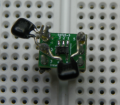
My estimation is that this type of layout is a complete and utter disaster,
but what do I know, it might be common practice.
Some things just can't be expected to perform correctly when
implemented in this "patchwork" fashion.
I estimate that You may never get this project to operate reliably in this form.
I think You will be chasing your tail trying to diagnose "the next" problem.
This is one of the reasons that I don't think much of SMD Devices when it comes
to "Maker-Projects" or DIY / Hobbyist type projects that will never be
put into Commercial-Automated-Mass-Production.
This Project would be easier to implement on a Large Perf-Board,
with mostly Through-Hole-Parts.
Figure on designing 2 or 3 or more proper, professionally manufactured,
Multi-Layered, SMD Circuit-Boards,
before You end up with a reliable product.
But remember,
I may have no-clue of what I'm talking about,
this is just my take on it,
and more experienced People should be consulted.
There are plenty here, and I'm sure they will chime-in.
.
.
.
Attachments
-
22 bytes Views: 4