Latching RC Circuit

Thread Starter

Ayden1717

Joined May 17, 2022
7
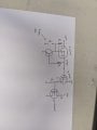
I am currently in the process of designing a circuit that will latch an input (at the latch set push button), then maintain a high output to the right side of the circuit so that the RC can charge and provide a high signal to the right-most N Channel until the capacitor is fully charged then goes low. Here is what I have so far.

I am stuck I believe because when I try to insert LEDs to provide me an indication of the state of the output (i am building in tinkercad), I believe it's messing up some of the connections... not sure if this is the issue or I am not doing this correctly. Let me know what I can change here!
 

Attachments

dl324

Joined Mar 30, 2015
16,839
Welcome to AAC!

For those who don't read sideways well:
1652833512485.png

How's the P channel MOSFET supposed to form a latch? As soon as the switch opens, the MOSFET turns off.
 

AnalogKid

Joined Aug 1, 2013
10,986
Please re-post the image with the correct rotation. Also, add a unique reference designator (R1, R2, Q1, Q2, etc.) to each component. We cannot discuss how a particular component behaves if it takes 5 posts to figure out which one we are talking about.

ak
 

LowQCab

Joined Nov 6, 2012
4,022
It would be very helpful if You would state what You are trying to accomplish as an end result,
as well as values, like Voltages, Currents, Time-Frames,
please be specific in describing what You expect the Circuit to do.
.
.
.
 

Thread Starter

Ayden1717

Joined May 17, 2022
7
Welcome to AAC!

For those who don't read sideways well:
View attachment 267424

How's the P channel MOSFET supposed to form a latch? As soon as the switch opens, the MOSFET turns off.
Please re-post the image with the correct rotation. Also, add a unique reference designator (R1, R2, Q1, Q2, etc.) to each component. We cannot discuss how a particular component behaves if it takes 5 posts to figure out which one we are talking about.

ak
Hi I apologize for the incorrect orientation here is the better one with the reference designatorsPXL_20220520_225948178.jpg
 

Thread Starter

Ayden1717

Joined May 17, 2022
7
The goal of this circuit is to essentially provide a high signal to the load R4 from Vdd for a limited amount of time (based off of RC constant) then once the capacitor C1 becomes charged it will then shut off the MOSFET Q4. In this case then the switch SW1 must perform a latch as an input signal in order to keep Q3 conducting indefinitely (until power is removed).

This circuit is for a ready to drive sound on an electric vehicle, once a certain event is triggered (in our case a push button), we need to have a buzzer sound for 1-3 seconds (must use hard electronics no microcontrollers), and this is the only way I could think of to do it.

My thought process of this circuit is as follows;

The switch SW1 pulls the gate of the P-Channel MOSFET low enabling it to have the output go high which then latches the output by driving the base of the N-Type BJT (Q2). Once this output remains high it will then allow charging of the capacitor C1 which will allow Q4 to conduct until the capacitor is charged.

I hope this helps i apologize for the wrong photo orientation.
 

AnalogKid

Joined Aug 1, 2013
10,986
Q1 still is backwards.

C1 still needs a resistor from the Q3 source to GND to discharge it.

What is the load current through R4?

An additional resistor from the Q2 base to GND will assure a fast and crisp turn-off. This can be 10x R2.

ak
 
Q1 still is backwards.

C1 still needs a resistor from the Q3 source to GND to discharge it.

What is the load current through R4?

An additional resistor from the Q2 base to GND will assure a fast and crisp turn-off. This can be 10x R2.

ak
Little confused, the purpose of R3 is to provide a return path for C1 after it has been fully charged. Does the logic of the circuit make sense since we are unable to recreate it on Tinkercad. At the moment we are also unsure of the precise load current that will be going through R4.
 

crutschow

Joined Mar 14, 2008
34,280
Little confused, the purpose of R3 is to provide a return path for C1 after it has been fully charged.
It's not the bottom of the capacitor that's the problem, it's the top.
Once Q3 charges C1, there is no return path to discharge C1 at Q3's source, as Q3 cannot conduct current in the reverse direction in that configuration.
 

eetech00

Joined Jun 8, 2013
3,856
The goal of this circuit is to essentially provide a high signal to the load R4 from Vdd for a limited amount of time (based off of RC constant) then once the capacitor C1 becomes charged it will then shut off the MOSFET Q4. In this case then the switch SW1 must perform a latch as an input signal in order to keep Q3 conducting indefinitely (until power is removed).
Will this work for you?

When the button is pressed, the load energizes, and C1 begins to charge.
As C1 charges, the "RC" will fall below 0.7v, turn off the BJT and de-energize the load.

1653102132527.png
 

AnalogKid

Joined Aug 1, 2013
10,986
I would like to see a series of simulated switch bounces added to your circuit in the random fashion that they occur?
Won't matter. The circuit uses positive feedback to latch on the first negative-going transition at the gate of M1. After that, the switch can do anything and it will not affect the circuit output. The only requirement is that the switch be open at the end of the timing period.

ak
 

AnalogKid

Joined Aug 1, 2013
10,986
Little confused, the purpose of R3 is to provide a return path for C1 after it has been fully charged.
Nope.

R3 is there to create current path for C1 while it is being charged, the R-C turn-off delay for Q4. It also keeps the gate-source structure at a low impedance when the circuit is off, protecting Q4 from ESD.

The problem is that when the circuit is off (no Vcc), the top end of C1 is floating. There is no current path to discharge it. Depending on the part and the application, it can stay charged until the next time power is applied and the button is pressed. In this case there will be no delay period, and Q4 might not turn on at all.

A resistor in parallel with C1 will solve this, but it also will affect the timing period. A resistor from the top of C1 to GND (call it R5) will act to discharge C1 through R3 when power is off, but not affect the timing when power is on. To calculate the size of this added resistor, first determine the minimum time the circuit will have to reset itself between usage cycles. IOW, the minimum time power will be off before being reapplied (not the time between button presses). R5 is calculated using one of these equations:

Toff = 3 x (R3 + R5) x C1 >> C1 is discharged from 100% to 5%

Toff = 5 x (R3 + R5) x C1 >> C1 is discharged from 100% to 1%

ak
 

k1ng 1337

Joined Sep 11, 2020
940
Won't matter. The circuit uses positive feedback to latch on the first negative-going transition at the gate of M1. After that, the switch can do anything and it will not affect the circuit output. The only requirement is that the switch be open at the end of the timing period.

ak
How can Q1 turn on if the 'bottom' plate of the capacitors charges to -12V? I don't see a direct connection to the positive rail. I suspect the secret is relative potential of the base emitter junction.

The RC node is shown as +12V but wouldn't it be opposite the charge applied on the other plate?
 
Last edited:

AnalogKid

Joined Aug 1, 2013
10,986
How can Q1 turn on if the 'bottom' plate of the capacitors charges to -12V? I don't see a direct connection to the positive rail. I suspect the secret is relative potential of the base emitter junction.

The RC node is shown as +12V but wouldn't it be opposite the charge applied on the other plate?
There is no -12 V anywhere in the circuit. At turn on there is 0 V across C1. Q3 is off and R3 has the cap at GND potential. When Q3 (with the correct orientation) turns on, both sides of C1 snap up to Vcc, turning on Q4. C1 then charges "up" through R3. After 3 time constants, the top of C1 still is at Vcc, while the bottom is 95% of the way to GND, way below the Q4 threshold voltage, turning it off.

ak
 

k1ng 1337

Joined Sep 11, 2020
940
There is no -12 V anywhere in the circuit. At turn on there is 0 V across C1. Q3 is off and R3 has the cap at GND potential. When Q3 (with the correct orientation) turns on, both sides of C1 snap up to Vcc, turning on Q4. C1 then charges "up" through R3. After 3 time constants, the top of C1 still is at Vcc, while the bottom is 95% of the way to GND, way below the Q4 threshold voltage, turning it off.

ak
I was referring to eetech's example.
 

eetech00

Joined Jun 8, 2013
3,856
I was referring to eetech's example.
Initially, there is a path to ground thu R2, R3 (these are bypassed when Q1 turns on). When the button is pressed, C1 momentarily appears as a short circuit, and this is what turns on Q1. C1 continues to slowly charge up. The voltage at "RC" contiually drops (as C1's impedence get larger) until its below Q1's Vbe threshold (0.7v). When below 0.7v, Q1 turns off. If the button is held down past the timing period, then the output will remain energized. Otherwise, it will quickly discharge thru the load, or, as AK states, an additional resistor can be used to discharge C1. Switch bounce is not an issue since the circuit latches at M1's initial turn on.
 
Top