Just some general questions about remaking something from the past

Status
Not open for further replies.

Thread Starter

Berzerker

Joined Jul 29, 2018
623
Yea sorry MrChips and AG I had a lot on my plate yesterday. I'm tearing down and re-building a porch on my house, had company come by, We barbecued and I have to admit we had a few "ice cold adult beverages" which I don't do very often. so I kinda wasn't looking very good...o_O
 
Last edited:

Audioguru

Joined Dec 20, 2007
11,248
I used huge capacitors like the Jameco one 56 years ago in a vacuum tubes amplifier. The Epcos ones I have been using for about 40 years are much more modern, have better tolerance and are smaller.
 

Audioguru

Joined Dec 20, 2007
11,248
Again, you picked the wrong value, this one is 0.022uF but you need 0.22uF. 0.022uF will produce no low frequencies.
Since your radio voltage will be only 15V then look at the DC voltage rating and select at least double. 50V or 63V is fine.
 

Thread Starter

Berzerker

Joined Jul 29, 2018
623
your right AG I didn't catch the extra (0) in that. still drinking coffee to clear my head.
I have corrected this. Thanks for the heads up. Don't think I will do that again for awhile. Shouldn't have done it at all.
But it was fun while it was happening ….:D ….:cool:
 

Thread Starter

Berzerker

Joined Jul 29, 2018
623

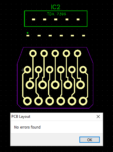
OK I'm trying to make my first PCB but I got some questions.
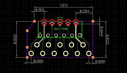
1. What are the red circles at the top where the through holes are?
2. notice there are only 6 pick points on the board outline, I want 8. I want the board to look like the top left corner does.
How do I add them?
Edit: found out to add the pick points
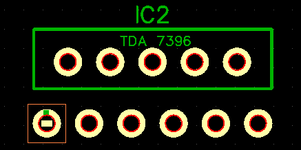
3. I made my holes round for the IC but the pins are square is this OK?
4. I want the holes where the IC is to solder on the bottom but I want the 11 holes at the bottom to solder from the top.
How do I tell which side gets soldered to and how do I change the bottom 11 pins to solder on the top?
 
Last edited:

ebeowulf17

Joined Aug 12, 2014
3,307

OK I'm trying to make my first PCB but I got some questions.
1. What are the red circles at the top where the through holes are?
2. notice there are only 6 pick points on the board outline, I want 8. I want the board to look like the top left corner does.
How do I add them?
3. I made my holes round for the IC but the pins are square is this OK?
4. I want the holes where the IC is to solder on the bottom but I want the 11 holes at the bottom to solder from the top.
How do I tell which side gets soldered to and how do I change the bottom 11 pins to solder on the top?
1.) DRC, or design rules check. The DRC makes sure you don't have traces, holes, or pins too close to each other, among other things. All of the DRC settings can be configured to your tastes, because each PCB manufacturer has different design limits. As a beginner, you could probably safely use the default DRC settings and be fine for years. If it says something is wrong, it probably is. Read the manual about DRC results and settings. I think you can click and/or right click the circles to find the error, but I'm not sure. There's also DRC stuff in the drop down menus.

2.) Read the manual. It'll tell you how to modify the board outline. It might be right clicking the outline to add a point, but I'm not sure.

3.) That's fine. Just make sure your hole diameter is larger than the diagonal measurement across the square pin, not its length or width alone. You also want some clearance between the two. Tons of articles online discussing how much larger the hole should be, beyond pin size. Read on.

4.) Check the documentation. In my older version, there's a tiny drop down menu near the top-right of the interface which lets you choose top side or bottom side.
 

Thread Starter

Berzerker

Joined Jul 29, 2018
623
Thanks ebeowulf. And just like the pattern editor and the component editor I seem to find out how to mess things up right off the bat.
Hit the DRC button on that PCB in post #393 and There were about 50 to 60 errors. There were so many red circles it looked like a red circle board. Started hitting google, the help section in diptrace, the diptrace forums and "anything" I could find. So I decided to step back and look at everything I done, the component itself and the pattern and how I laid out the board. left a field in the pattern editor where it says pin diameter at a "value" where there shouldn't be cos their are no holes in the pins on the IC itself, their .020 X.037. So I redone the pattern and got it down to 22 errors. reading on one of them was a drill size error (?). I haven't seen or found a drill size button anywhere or where to put in a value or size.
Found something on it where I need to import them and hit the import button to import the drill sizes "it only listed one" .055. there are two different size holes on the board that need to be drilled. Reading on I seen it said you can add them (?). I looked and looked in the dialogue box and don't see, can't find and don't know how to add anything in this box. It also listed a pad error under each drill error. How can their be a pad error (?).
The pads are now correct and I double checked the spacing and all. running on about 8:30 or 9:00 last night feeling flustrated I done the dumbest of all "I hit the export button by mistake". Note to anyone who reads this: "DO NOT" hit the export button for any reason what so ever(!)
I lost ever thing don't know how to undo it, So I got up and left it for this morning to figure out.
Edit: Oh yea hit the auto button in the dialogue box where it was suppose to automatically add the drill sizes " from what I understood" It did nothing.
 
Last edited:

ebeowulf17

Joined Aug 12, 2014
3,307
Thanks ebeowulf. And just like the pattern editor and the component editor I seem to find out how to mess things up right off the bat.
Hit the DRC button on that PCB in post #393 and There were about 50 to 60 errors. There were so many red circles it looked like a red circle board. Started hitting google, the help section in diptrace, the diptrace forums and "anything" I could find. So I decided to step back and look at everything I done, the component itself and the pattern and how I laid out the board. left a field in the pattern editor where it says pin diameter at a "value" where there shouldn't be cos their are no holes in the pins on the IC itself, their .020 X.037. So I redone the pattern and got it down to 22 errors. reading on one of them was a drill size error (?). I haven't seen or found a drill size button anywhere or where to put in a value or size.
Found something on it where I need to import them and hit the import button to import the drill sizes "it only listed one" .055. there are two different size holes on the board that need to be drilled. Reading on I seen it said you can add them (?). I looked and looked in the dialogue box and don't see, can't find and don't know how to add anything in this box. It also listed a pad error under each drill error. How can their be a pad error (?).
The pads are now correct and I double checked the spacing and all. running on about 8:30 or 9:00 last night feeling flustrated I done the dumbest of all "I hit the export button by mistake". Note to anyone who reads this: "DO NOT" hit the export button for any reason what so ever(!)
I lost ever thing don't know how to undo it, So I got up and left it for this morning to figure out.
Edit: Oh yea hit the auto button in the dialogue box where it was suppose to automatically add the drill sizes " from what I understood" It did nothing.
Was there an error number or a better description for the "drill size errors" or "pad errors?" Not sure what those would be referring to.

It's interesting to me that there just a few circles before DRC, and lots after. I assume the first ones were also DRC indicators, but not sure why it would automatically show some while you worked, but wait until you requested DRC on others. Very odd.
 

Thread Starter

Berzerker

Joined Jul 29, 2018
623
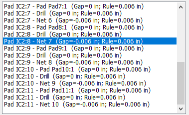
Just got back to it. errors
Pad Pad1:1 - Pad IC2:1 (Gap = 0 in; Rule = 0.006 in.)
Drill - Pad IC2:1 (Gap = 0 in; Rule = 0.006 in.)
I have tried increasing the hole size in the pads, changed them in the pattern editor and still get these errors.


Got the bottom 11 pads with no errors but now there's a shifted via (may break drill) error. What gives with that ? haven't moved anything. why would the drill move ?
 
Last edited:

bertz

Joined Nov 11, 2013
327
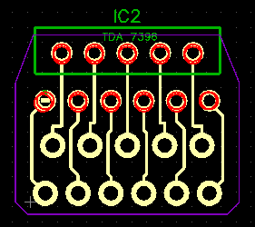
Here's better look at everything
....... error list...…...

Now if I move the IC I get this
You cant just move the IC without moving the hole pattern.
Have you created a component called TDA7396 and stored it in your custom component library?
Have you created a pattern for the TDA7396 and stored it in your custom pattern library?
Have you linked your component to the pattern?
 
Status
Not open for further replies.
Top