Is the 5i22 board going to drive an existing motor board, and if so, what is it?
Now we know the 5i22 controller chip outputs will be active low. All that is needed is the motor driver board info.
Is the 5i22 board going to drive an existing motor board, and if so, what is it?
Now we know the 5i22 controller chip outputs will be active low. All that is needed is the motor driver board info.
As you say, we know the 5i22 controller chip outputs will be active low. Now I'm trying to figure out the info about the stepper driver that needs 24V signal. As I need to convert the 5V from the 5i22 to that 24V, I have to determine if I need isolation to use optocouplers.Conversely, I would use 74LS07 for the level shifting.
5. That's what I have to be clear if I need isolation. I don't have enough information about the stepper driver to determine if I need isolation. If isolation wouldn't be required I would just use a 74LS07 for level shifting.
Normally you should not need isolation if you take all power commons to a common star point, also if using a P.C./5i22 combo, the P.C. power is connected to earth ground in the P.C.
Max.
I modified the circuit as below, so you still can use high(1) as control signal, the output pin was connected to input of 5i22, the I/O of 5i22 was connected to the resistor and pull high.
I modified the circuit as below, so you still can use high(1) as control signal, the output pin was connected to input of 5i22, the I/O of 5i22 was connected to the resistor and pull high.
But that is active high input, isn't it? But as stated above it should be active low, so the I/O pin should be connected to the cathode of the LED, correct me if I'm wrong or I'm misunderstanding your schematic
But that is active high input, isn't it? But as stated above it should be active low, so the I/O pin should be connected to the cathode of the LED, correct me if I'm wrong or I'm misunderstanding your schematic
Yes, that is active high and the output was low to the I/O of 5i22, so it was matched the required what the states of 5i22 that I posted in #20, the input to output just like an inverter, but the output is an open drain.
Let's assume isolation is require (and it probably isn't, but ...) and start at the output.
We'll assume that the input being driven by the circuit requires no current when the input is either high or low. This is unlikely to be true, but as we'll see we can probably account for it with a minor change.
If we don't have to supply any input current to the driver board, the 1k resistor is probably a lot lower in value than necessary. The current through it will be roughly 24 mA with a 24 V supply, which is rather a lot, but we'll leave it at that value for now.
Turning to the 2N3904, we would like to know how much base current is required to control that 24 mA of collector current, so we need to look at the datasheet for the transistor. We'll use the sheet from ON at https://www.onsemi.com/pub/Collateral/2N3903-D.PDF. In the sheet there is a table titled ON CHARACTERISTICS. There we find a spec of a minimum gain of 60 for 50 mA of collector current with 1 volt collector to emitter, and 100 at 10 mA. Farther down we find collector-emitter saturation voltage which is spec'd with 5 mA of base drive for 50 mA of collector current. This is an "overdrive" condition, typical of the way saturation is specified. To decide is saturation is required we would have to have a spec for the inputs of the driver board. Chances are that a LOW input doesn't need to be that low if the signal must swing up somewhere near 24 volts for HIGH. Now let's look at Figure 15, which is typical DC current gain. We see that the typical gain is much lower at -55°C than at 25°C. Normally, you don't use typical values for design purposes, but use the the maximum and minimum values from the tables - and the graphs are "normalized" so we still need the tabular data. Figure 15 says that we can expect the current gain to be about half as much at 30 mA at -55°C as it is at 25°C. Let's say we need to operate to -55°C, and we won't go to full saturation, but allow about a volt across the transistor.
So, if we take the table minimum gain of 60 at 25°C and apply a factor of 0.5 to run at -55°C, we can expect a minimum gain of about 30. Let's be conservative and say we'll get 20, even though we are already using the minimum. Assuming 20 gives us some additional margin. If we get too carried away with adding margin we get into "it can't be done" territory, when it can be done.
So, for a current gain of 20 and 24 mA of collector currrent we should have a base current of 1.2 mA, which brings us to R4 and how we pick that value.
coupler datasheet: http://www.sharp-world.com/products/device/lineup/data/pdf/datasheet/pc817xnnsz_e.pdf
First, we'll deal with that leakage current issue, which is also rather complex if you look at all the details. The base cutoff current from the datasheet is 50 nA max, which is "nothing". The coupler output OFF ("dark") current will likely be considerably higher. From the graph (Figure 11 of Sharp datasheet) we get up to 1 µA at something over 90°C. Let's be extra conservative and assume it will actually be twice as high. We know that a silicon transistor has a base-emitter voltage in the range of about 0.6 V when conducting, but we also know that some current can flow at lower voltage. Without belaboring the details, let's aim for a maximum of 0.3 V at 2 µA, equating to 150k ohms. If we say Vbe will be 1 volt when the transistor is being driven hard, we would be putting 15 µA through that resistor, which is not much especially compared with the 1200 µA we want for the actual base drive. If we used only 10k, the current through it at 1 V would be 100 µA. [EDIT]: That resistor also improves the turn-off speed of the 2N3904 by allowing some path for removal of carriers from the base region, rather than simply allowing them all to recombine. 10k won't make a big improvement.
R3 is the resistor that limits the base drive current, which we said needs to be 1.2 mA for the base, and let's use 0.1 mA for the base-emitter resistor, so we need 1.3 mA. The coupler datasheet isn't too great, so we'll look at the graphs and be extra conservative. The curve for 5 mA of collector current in Figure 8 is almost flat over a wide voltage range. Let's assume the collector-emitter voltage will be 5 volts at 5 mA - it we look at the other curves, this gives us some flexibility on the input side. So, 1.3 mA with (24 - 5) V means R3 should be about 14.6 k ohms. Let's set R3 to 10k. We've already been extra conservative and could use say 15k, which is also a common value, but we decided to use 10k base-emitter for the 3904, so let's not add another value of resistor to the bill of materials. If we assume that 100% of the supply voltage will be applied across that 10k resistor, we get an optocoupler output current of 2.4 mA.
NOW to the input. We need 2.4 mA from the output, so we need to determine the drive current for the input. From the Electro-optical Characteristics table, we find a line saying we can expect a minimum of 2.5 mA at 5 V Vce with 5 mA of input - at 25°C. Always that blasted 25°C spec. Figure 9 actually has a curve for that 5 mA, 5 Vce value, showing that the transfer ratio drops to about 65% (normalized!) at 90°C. We probably should put 5 mA/0.65 = about 8 mA into the emitter. I was hoping it would be much less.
The calculation for R2 is fairly straight forward, but if "PIN 49" voltage is 5, 330 ohms is going to be about right (5 V - Vf for IR emitter - 5i22 output low voltage)/8 mA.
This whole chain of calc's has been quite conservative at every step. The only thing still missing is the degradation in the optocoupler's emitter performance with aging. The datasheet is not helpful. The lower the current, the lower the degradation rate. The absolute maximum input current is 50 mA, and since we are putting in substantially less we probably have a low aging rate.
Note Figures 13 through 16 which describe speed performance. If there is a need for speed, then keeping R3 at 1k will be helpful. Otherwise, revisiting the value of R3 as the pullup, with the aim of reducing it, may allow lower input drive to the coupler. Conversely, if the 2N3904 needs to sink current from the driver board input at logic LOW, then more drive may be needed.
A small-signal MOSFET could be an improvement over the 2N3904, allowing reduction in the requirement for current in the coupler output - but then that speed thing comes in again. The speed will be almost 100% limited by the optocoupler performance and not by the effect of the input capacitance of any small FET.
As is apparent, using an optocoupler makes the details surprisingly complex. If you don't need isolation, don't use it, but do pay attention to managing voltage drops in circuit commons ("ground"). That can also be quite a pain, depending on system architecture.
You must be careful with active-low outputs in some cases where it is possible for current to flow into the output of an IC when the IC is not powered. This will almost always be the case with totem-pole outputs and certainly the case where the output has a protection diode to the IC's positive supply rail. If the output is open-collector or open-drain and the diode is not present, it is usually safe.
Where you are concerned with system safety and even the very brief transients can't be tolerated, special methods should be considered that will prevent the unwanted transients. This may include careful sequencing of power supplies at startup and shutdown or addition of interface ICs that can be held in a condition of well-defined output state during startup and shutdown. With a microcontroller, sometimes you can do things like using two outputs to enable the power devices - one output passively pulled low, one passively pulled high, and both required to be in the state opposite to the passive pulling to enable.
Good power supply supervisory circuits are, like the optocoupler circuit, surprisingly complex.
In this post I have attached the datasheet of a stepper driver similar to the one that I will use. The difference is that this one works with 12V signal. Mine have to work with 24V for the step an direction signal.
That board is for active High inputs. And the output is 24V max.
For a sec I thought, "Wow! That is expensive" then noticed it was not $. The price works out to be under $3.00 so that is better.
I modified the circuit as below, so you still can use high(1) as control signal, the output pin was connected to input of 5i22, the I/O of 5i22 was connected to the resistor and pull high.
No.
The opto and its resistor need to be parallel to the blue LED.
Then, as you are driving 2 LEDs, check the processor's current sink capability to make sure you are not overloading it.
You should reversed the D2 LED and connected the negative pin of LED from pin 49(Power) to Pin 50(GND), you also don't need the R2, because it was connected to the pull high resistor in the I/O of 5i22 and I already mentioned it in #24
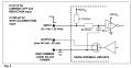
Image 1 shows different configurations that the manual recommend.
Image 2 shows the signals explanation that I mind, step and direction
Image 3 shows the input configuration of the driver.
According to that, I think now I have to modify the circuit. But the concept of open collector still remains.
Unless there is a need to heavily load the optocoupler output for speed or there is a need for logical inversion, drive the inputs directly with the optocoupler outputs as current sinks (i.e. common emitter) and reduce the drive to the coupler input by a factor of 2 or 3.
Note that the words "low impedance source" are misleading - it needs to be a low impedance sink and there is no need to source any current to the inputs.
If there is a need for inversion, I would consider a transistor array such as one of the ULN200x series or some other driver IC rather than a whole handful of discrete resistors and transistors.
The new circuit just as a buffer not as an inverter, so when a low signal input from I/O pin then the stepper driver will be activated, the active signal of stepper drive is from high to low, so the stand by voltage level is high, how do you setup the input signal from I/O pin that it will affects the input of stepper driver.
As your present circuit, after the system reset then the input of stepper driver will be pull high to waiting for a low level to active, and if you want to keep the led of photocoupler at a high level then what will be happens of stepper driver when the I/O pin is at the low level?
 Facebook
 Google
 GitHub
 Linkedin