Facebook
 Google
 GitHub
 Linkedin
Hi all,
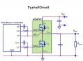
I want to use IR2110 for driving two MOSFETs (IRFP22N60K) & I connected it with mosfet like this:
i fed the Hin pin with noninverting PWM signal, and inverting PWM signal for Lin pin generated by 555 timer.
For bootstrap capacitor, i use 470nF ceramic cap and 1N4148 diode between pin 3 & pin 6.
But the problem is The mosfets are not working as switch.
Help me out with solution.
Thanks in advance
Attachments
-
 176.3 KB Views: 211
")