IR2110 Functional Block Diagram

Thread Starter

BlackMelon

Joined Mar 19, 2015
173
Hello,

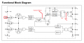
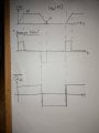
The block diagram is on the IC's datasheet. Let Vdd = 5V, and Vss = 0V. After the IC has been disabled (SD=high), I fed a square wave (5V/0V) to HIN pin. When the square wave is low, will this cause an ambiguous Q of the upper SR-flip flop? If so, will it ruin the operation of the IC?

About the pulse gen block, why do we have to have it? Will its upper and lower outputs be in-phase with the output of the upper NOR gate?

Thank You
BlackMelon
 

AlbertHall

Joined Jun 4, 2014
12,623
When SD is high, the flip flop S pin is asserted so it is held in the SET condition.
For more read section 2.1 Input Logic in the link below.
For the Pulse Gen read section 2.3 High Side Channel here.
 

Thread Starter

BlackMelon

Joined Mar 19, 2015
173
When SD is high, the flip flop S pin is asserted so it is held in the SET condition.
For more read section 2.1 Input Logic in the link below.
Please note that the block diagrams in the app note AN-978 and in the IR2110's datasheet are different from each other.
Have you forgotten about the HIN pin? According to the IR2110's functional block diagram, if one uses a microcontroller to control a half-bridge converter, when the MCU detects failures, the user might signal "high" to the SD pin, so we have S="high". However, at the HIN pin, if there is still "high/low" square wave incoming, when the wave is high, we have S=R=high, which is a forbidden state of an S-R flip flop.


For the Pulse Gen read section 2.3 High Side Channel here.
In the section 2.3 High Side Channel, could you explain the sentence "As shown in Figure 2 the on/off commands are transmitted in the form of.......of the input command"? If I apply 5V-0V square wave at the HIN pin, how will the "narrow pulses" look like? And what is the "on-off command"?
 

AlbertHall

Joined Jun 4, 2014
12,623
The diagrams differ because the pdf refers to a 'generic' driver.
What happens when both SET and RESET are active depends on the design of the flip-flop - it may force the SET or RESET condition or it may be undefined. For this chip, it forces the SET condition.
The on/off commands is the signal from HIN and, as described, will be narrow pulses.
 

Thread Starter

BlackMelon

Joined Mar 19, 2015
173
For this chip, it forces the SET condition.
Is there any point in the app note saying in this way? I just want to know cuz I have spent days searching for that condition.


The on/off commands is the signal from HIN and, as described, will be narrow pulses.
And about the "narrow pulses at the rising and falling edges of the input command", suppose that I input a signal to HIN like in the attachment. Will the narrow pulses be like this?
Will it come out of the pulse generator?
Will it make the latch "A" have the QA-bar output like what I have sketched?
 

Attachments

Thread Starter

BlackMelon

Joined Mar 19, 2015
173
Yes, except I would expect the pulses will all be positive going.
Yes there are possibilities of either the case. I don't want to reverse engineer IR's chip, so I will not go any deeper. I just want to know how the chip function + some background details. Anyway, thank you everybody for helping me through a rough reading of the IC's datasheet. :)
 
Top