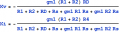
It has to contain Rd because the expression for Kv contains Rd.
If you know the input impedance of the amplifier to be R4 ohms, and if the load in which you want to reference the current is Rd, then you proceed follows:
The input current is Iin = Vin/R4; the output current is Iout = Vout/Rd.
This multiplication of Kv by (R4/Rd) causes the Rd in the numerator of the Kv expression to be replaced by R4, which you got, but the denominator should remain the same (includes Rd, in other words).
How did you calculate Ki? What assumptions and equations did you use?
Your reasoning makes sense. I didn't calculate Ki in paper. I used the software snap. http://snap.webpark.cz/indexa.html
Don't know why this software give the incorrect result.
This circuit is too complex and it took me a lot of time with no result. Finally I decided to use the software.
I think your method to calculate Ki is right.
At a frequency that high you definitely need to provide a capacitor to ground from the gate of M2--a capacitor suitable for use at 1.7 GHz!
I found the circuit in a book in which R1 is a capacitor. In my view, this capacitor is what you meant.
(the capacitor will connect gate to ground if Rs is very small.)
I am not sure about this. In contrary, I think SNAP has calculated correctly.
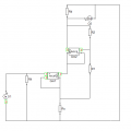
The "out" symbol is connected to the output of an ideal current source - and I cannot see how Rd should influence the output current.
On the other hand, the current through R1 and R2, of course, DOES influence (via feedback) this current.
Snap may have calculated correctly, but, of course it can only calculate what it is programmed to calculate.
Assuming that Ki is the ratio of the current in Rd to the input current, Snap (or any other software) should be able to get a correct result. That's why I asked anhnha "How did you calculate Ki? What assumptions and equations did you use?", because if he got a wrong result, he must have set up his equations incorrectly.
The "out" symbol is connected to the output of an ideal current source - and I cannot see how Rd should influence the output current.
On the other hand, the current through R1 and R2, of course, DOES influence (via feedback) this current.
If Rd were the only thing receiving the output current from the ideal current source, then the current in Rd would not be affected by the value of Rd.
But, since there is another resistor connected to the output node (R1 in Jony's circuit; R2 in anhnha's circuit), the fraction of the current from the ideal current source which passes into Rd depends of the value of Rd.
I think, the problem is that the "out" symbol can be used unambigiously for voltages (across the symbol) - but, on the other hand, it is not quite clear which current is defined as "out".
Three alternatives: Current through RD, through R2 or out of the source.
(At least, it is not clear to me. What do you think?)
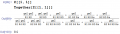
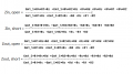
You probably saw the same result I did when I looked at Z[[1,1]] with the Shekel method. But after using the "Together" command, I got the result I expected for Zin:
I think, the problem is that the "out" symbol can be used unambigiously for voltages (across the symbol) - but, on the other hand, it is not quite clear which current is defined as "out".
Three alternatives: Current through RD, through R2 or out of the source.
(At least, it is not clear to me. What do you think?)
As I said, if it is assumed that it is the current through Rd, then the value of Rd affects the current gain; if it is assumed to be the current out of the source, then Rd has no effect on the current gain.
Usually in the problems posted by students on this forum, the current gain is taken to be in relation to the current in some specific load resistance.
anhnha should tell us what the definition of Ki is for this problem; what is taken to be the output current. I took it to be the current in Rd. The values of R1 and R2 should probably be quite large compared to the value of Rd, so Rd is the effective load.
Of course, as Jony mentioned, this is an analysis of a low frequency circuit and is not applicable to a 1.7 GHz circuit.
Yes, output current is the one flowing through Rd. That is what I think the software will choose. I have just used it and don't know much about it. With the input and output as in the picture. I change how output is measured and get the same result for Ki.
Do you mean that you get the same result that you got in post #38, or do you mean the "same result" as I got (with Rd in the denominator).
If you mean the same as you got in post #38, you'll have to show how you set the equations for Snap to solve if you want us to help determine why Snap doesn't give a result with Rd in the denominator.
If you mean the same as you got in post #38, you'll have to show how you set the equations for Snap to solve if you want us to help determine why Snap doesn't give a result with Rd in the denominator.
I wanted to do that but I can't see any equations in snap. The only thing I need to use this software is to take components and arrange it as in the picture. Then I only need press the Ki button and get the result. No equations and how it is calculated are visible.
I need to find out how the output current is defined in snap. I tried another software but there is no calculation of Ki.
EDIT: It is a bad situation that the DIRECTION of the output current source is not shown on the display - however, after consulting the pdf-manual I`ve got the impression that for both VCCS elements the feedback path is incorrect (circuit in post#52).
But without R4, the input impedance is just the gate of a FET, and that input impedance (at low frequency, which is what we're doing) is infinite, leading to an infinite current gain if R4 is actually removed from the circuit. I think the numerator of the current gain expression needs to have an R4 term.
I explained in post #44 why there should be an R4 term in the numerator of the current gain expression.
Yes - I have noticed it. However, probing of a current is more logical (if compared with SNAP) and - as mentioned already - the direction of the VCCS output current is indicated.
However, everybody will have his own preference.
Regarding R4: I am afraid, you misunderstood my remark. Of course, I mean "eliminated" in the equation - not in the circuit. Or did you assume I would consider a parasitic FET input current as an input for defining a current gain?
But what do you think about my remark concerning VCCS feedback in the SNAP diagram?
Regarding R4: I am afraid, you misunderstood my remark. Of course, I mean "eliminated" in the equation - not in the circuit. Or did you assume I would consider a parasitic FET input current as an input for defining a current gain?
I understood what you meant by "eliminated" from the equation. But then there would be no R4 term anywhere in the expression for Ki. My further remarks were to suggest why it would seem that there must be an R4 term in that expression. R4 is what determines the input current; without it there would be no input current (other than a parasitic current).
What I'm suggesting is that the expression for Ki you got with SAPWIN isn't correct. In post #44 I explained how to derive an expression for Ki when the expression for Kv is known, and the input impedance and load impedance are known. Do you agree with my explanation as to why R4 should be in the numerator?
As you say, the direction of the output current is not shown, but I assume the + sign on the control side should correspond to the gate of a FET. That leads me to think that GM2 is oriented incorrectly, but without an output current direction shown, I can't really offer an opinion.

 Facebook
 Google
 GitHub
 Linkedin