I want to use a rotary knob to pulse resistance (2)

Thread Starter

impala454

Joined Apr 4, 2012
15
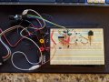
I realize this is an ancient thread, but I am attempting to build this exact circuit. I am going to control a pioneer car stereo head unit via its wired interface (a 3.5mm stereo jack). I have confirmed that putting a 16k resistor from tip to sleeve does volume down and 24k resistor does volume up. I am a software guy by day and thought about doing this with arduino, but also don't want foul ups to crank my volume way up so ended up finding this thread. I built the circuit as @AnalogKid shows above except I didn't have 2N7002's laying around so I used 2N7000s instead. I also think from my tinkering w/the arduino version that my pulses need to be at least 50ms or so for the unit to pick up. I tried many different C4 values and just can't seem to get this to work. I also have fairly limited understanding as to what the upper left part of the schematic is doing. Has anyone built this or something similar before? Hopefully this image of my terribly messy breadboarding will help.

<MODERATOR: Find the post referred to here.>
 

Attachments

Last edited by a moderator:

Thread Starter

impala454

Joined Apr 4, 2012
15
Yeah sorry it is messy. It should be exactly the circuit posted above by analog kid, with the exception that I replaced the 2N7002s with 2N7000s.
 

Thread Starter

impala454

Joined Apr 4, 2012
15
My main questions:
  1. Validation of the schematic above
  2. Is it ok to swap the fets like I did
  3. What value of C4 would get me a roughly 50ms pulse
  4. What the larger caps in the upper left part of the schematic are for
Thanks for any help!
 

AnalogKid

Joined Aug 1, 2013
10,986
1. Looks good to me.

2. Yes, The two part numbers use the same die. The only differences are the package and the power dissipation rating (which is not an issue in this circuit)

3. The output pulse width is *approximately* equal to 0.7 x R3 x C4.

4. C1 and C2 are power supply decoupling capacitors. They assure that the chip sees a near-zero impedance power source. This is critical for proper chip operation. C2 usually is a small ceramic cap, and should be placed as close as possible to the chip's power and GND pins, with short leads.

With a 50 ms pulse width, the trailing edge at pin 1 will be rising slowly. this might cause a noise burst at the gate output as it transitions from high to low. A solution uses the remaining gate (U1D) plus a resistor to create positive feedback around U1A, but that does not solve the problem for U1B. Try the circuit as is and see if there is a problem.

Another consequence of a longer pulse is the timing of the steering signal on pin 1 of the encoder. You might have to increase C3 to something line 0.47 uF.

ak
 

crutschow

Joined Mar 14, 2008
34,282
Below is the LTspice simulation of a circuit that uses one CD4013 D-FF chip to perform the decoding:
It is insensitive to switch bounce from the source.
The output (purple trace) goes to a lower voltage for the down pulses, indicating the 16kΩ resistor is being pulsed.

It's possible you don't need the R and C at the MOSFET gates to generate the pulses if the volume control can tolerate one resistor being continuously on when the volume control is static.

Edit: I didn't show 10kΩ pull-up resistors to Vdd on the the two inputs, but they will be needed if the encoder is a switch contact to ground.

Edit 2: Just realized circuit has problem with negative going switch bounce. Redesign in progress...


1660667786734.png
 
Last edited:

ebeowulf17

Joined Aug 12, 2014
3,307
I bow to the LTS master.
You shouldn't be bowing to anyone - you're a master in your own right and have contributed so much to this forum and to my personal understanding of electronics!

That said, crutschow is an amazing designer and teacher and deserves all the respect and praise in the world. He's also helped me, both directly and indirectly, on countless projects and taught me so much.

You're both just mind-blowingly knowledgeable and helpful. Can't thank you both enough for all your generous contributions here.
 

crutschow

Joined Mar 14, 2008
34,282
Spoiler alert. :eek:

After some further simulation of my post #6 circuit, I realized it was only insensitive to switch bounce on the signal rising edge, not the falling edge. :oops:

Redesign in progress---
 

AnalogKid

Joined Aug 1, 2013
10,986
After some further simulation of my post #6 circuit, I realized it was only insensitive to switch bounce on the signal rising edge, not the falling edge.
Not to hijack this thread (we can spin this off into its own), but speaking of that . . .

I picked up another circuit of yours, and have used it in posted designs (usually with credit). Then, one day, I built it. Uh oh.

It uses 1/2 of a CD4013 as a self-debouncing toggle flipflop. The problem is that it, too, false-triggers on switch release due to contact noise. Darn those pesky nanoseconds. I had to go back to something you have ding'd me several times for doing, shorting out a timing cap with the switch.

ak

Toggle-Dff.png
 

crutschow

Joined Mar 14, 2008
34,282
Yes, I didn't previously realize that switches could also bounce on release.
One of the dangers of simulation -- not using the proper model. :oops:
 

eetech00

Joined Jun 8, 2013
3,858
Not to hijack this thread (we can spin this off into its own), but speaking of that . . .

I picked up another circuit of yours, and have used it in posted designs (usually with credit). Then, one day, I built it. Uh oh.

It uses 1/2 of a CD4013 as a self-debouncing toggle flipflop. The problem is that it, too, false-triggers on switch release due to contact noise. Darn those pesky nanoseconds. I had to go back to something you have ding'd me several times for doing, shorting out a timing cap with the switch.

ak

View attachment 274030
A HEF4013B has a schmitt triggered CLK input....
 

crutschow

Joined Mar 14, 2008
34,282
Here's my circuit modified with an added Schmitt-trigger inverter and RC filter to suppress the effect of switch-bounce.

Using a HEF4013B with Schmitt-trigger clock inputs would eliminate the need for the inverters.

1660754388911.png
 

Thread Starter

impala454

Joined Apr 4, 2012
15
Wow I'd stopped receiving email notifications and thought the thread was dead. Thanks for all the replies!

crutschow said:
It's possible you don't need the R and C at the MOSFET gates to generate the pulses if the volume control can tolerate one resistor being continuously on when the volume control is static.
I think that is the case, as the arduino project I was modeling after just raised the resistance to the digitpot's maximum when the knob wasn't being turned. Here is that project for reference.

Thanks a lot for the ciruit! A couple of quick questions (apologies for silly questions as I only dabble in electronics and am a software guy by day):
  • The X and Y, are those my "A" and "B" outputs from my encoder?
  • The CD4013B seems to have a lot of variants, which one specifically would you recommend?
  • Same question on the CD40106B (and is there a recommended place to buy them? I do not mind doing the kits which contain many things as I may end up using the extras elsewhere)
  • Is the 13V input just to be easier to match the car or selected for another reason? I currently have the stereo hooked up to a bench supply for testing so no big deal either way. Do you think it'll tolerate directly being connected to the car's 12V supply or do I need to have something else in front of it?
 

Thread Starter

impala454

Joined Apr 4, 2012
15
impala454 said:
I think that is the case, as the arduino project I was modeling after just raised the resistance to the digitpot's maximum when the knob wasn't being turned.
Actually in re-reading this, I see what you were asking. No, if the resistance is there, it will continue to raise/lower the volume. E.g. if I just put a 16k or 24k resistor across the stereo pins, it will raise/lower the volume until I remove the resistor.
 
Top