I can't figure out how to drive an 8Ω load!!!

Thread Starter

babaliaris

Joined Nov 19, 2019
208
8ohm load design.png

Now that I understand Electronics, I tried to implement a simple "bad" sound amplifier to test my knowledge, and I found impossible to drive an 8Ω load without attenuating the signal!!!

The following are not exactly the real calculations, but close enough. I have changed some parameters (RC, and Rx bias), but the idea of the challenges is the same.

First I created the first stage at Q1 with Ic = 1mA and Vc = Vcc/2 = 10V. I immediately noticed that the requirement for Vc = Vcc/2 with a big RC, COMPLETLY resticts the voltage at the base!!! I had to use Vb = 1V, in order to achieve the 1mA current and Vcc=10V!

Challenge 1: Trade-off between base voltage and Vcc, current requirements!!! Because the input is only 5mV, for this case 1V in the base is enough to not cut off the transistor.

For the Rin calculations, I'm assuming that the parallel of the Voltage Dividers resistances is high enough (which it is) to approximately give the Rin without including them

I will also assume the min Hfe value of the transistors I have in my home, which is B=100.

Final results in the first stage:
\( gm_{1} \approx \frac{1mA}{25mV} = 0.04S \) \( \frac{1}{gm_{1}} = 25Ω \)
\( Rin_{1} \approx \frac{B}{gm_{1}} + (B+1)Ree1 \approx \frac{100}{0.04} + 101 \cdot 47 \approx 7.247k\Omega \)

Rin should be good enough, I do not expect high Signal input resistance (smartphone).

\[ Av_{1} = \frac{Rc}{\frac{1}{gm_{1}} + Ree} = \frac{10k}{\frac{1}{0.04} + 47} = 138V/V \]


Stage 3 Power Amp:
Of course, I can not drive the 8Ω load directly because RC//8Ω will give 8Ω and the gain will be reduced a lot!!!

First, I thought to add the power (common collector) amplifier Q3.

Challenges: Increasing the bias current of the power amplifier, results in a small Rin, which counterattacks the requirement of a Rin3 >> Rc = 10k!!!
Also, this time I need a bigger Vb3, because the output of the first stage will be bigger in amplitude!!!!

Increasing Vb3, results in an increased voltage drop in the RE3, which results in a bigger current or bigger RE3!!!

I choose to use a 50mA bias current which results approximately in an Rin3 = 860Ω!!! The good thing is that 1/gm3 gets really small, and the parallel resistance of RE3//RL does not change the unity gain that much of the power emitter follower.

So I thought, let's use that and use a Voltage Buffer in between what gives a big Rin2 >> Rc = 10K and Rout2 << Rin3 = 860Ω??

Stage 2 Voltage Buffer:
Now I can't make this voltage buffer to work...

Decreasing the bias current results in big Rin2, but in a BIG RE2 that destroys the gain in the third stage.

Also, requiring a big Vb2 =6.66V, increases the voltage drop at RE2 which also leads to a bigger RE2 that destroys the gain in the third stage
OR a bigger bias current that lowers Rin2 and destroys the amplification of the first stage...

I don't know what to do...

I decided to put Vb1 = 1v => RE2 = 1KΩ => IC2 = 1mA which gives Rin2 = 103.5KΩ but Rout = 1k > RIN3 = 860Ω that attenuates the third stage...

Conclusion:

It seems that analog design is actually much harder than I anticipated.

What should I do, to fix the above circuit?
 

Attachments

Last edited:

Jony130

Joined Feb 17, 2009
5,541
What goals did you want to achieve?
Have you tried to use a Darlington emitter follower? Maybe directly coupled?
1d.PNG

Also, notice that BC337 is not a power transistor, Q3 should have been a power transistor or medium power one.
 

Attachments

Last edited:

Ian0

Joined Aug 7, 2020
10,293
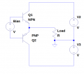
You need a push-pull design for the output stage, with a complementary emitter follower.
If you were to attempt it with a single-ended amplifier, then you would need RE3 to be much lower than your load impedance.Screenshot from 2024-05-27 17-53-04.png
 

Thread Starter

babaliaris

Joined Nov 19, 2019
208
What goals did you want to achieve?
Have you tried to use a Darlington emitter follower? Maybe directly coupled?
View attachment 323254

Also, notice that BC337 is not a power transistor, Q3 should have been a power transistor or medium power one.
Yeah, I haven't studied this configuration yet, so probably I tried to re-invent the wheel myself :p

I see how this works. You basically use DC couple to get the free DC offsets from the previous stages while the Ic2 of q2 is low, something like 0.28mA you get a really big Rin and Really small 1/gm2 rout (Actually, this will be something like 80Ω but this is still much smaller than 860Ω)!!!

While the third stage gives a current of 80mA, and an Rin that is small but definitely much bigger than 1/gm2!!!

Lol this is quite awesome!!!

I imagine the limit with these stages will be the 0.7 voltage drop at the base emitter? So If for some reason, I had to use more stages, eventually from VC1 all down to Vbn, where n the last stage, the last base will have such a small voltage that will lead to cut off.

You need a push-pull design for the output stage, with a complementary emitter follower.
If you were to attempt it with a single-ended amplifier, then you would need RE3 to be much lower than your load impedance.View attachment 323253
I need to study this, never seen this before. But I need a negative -VEE power supply as well. Which I do not have.
 

Ian0

Joined Aug 7, 2020
10,293
But I need a negative -VEE power supply as well. Which I do not have.
Not necessarily.
When drawn in isolation, it is clearer with positive and negative supplier what is does, but It will work with a single supply if you capacitvely couple to the speaker.
 

Thread Starter

babaliaris

Joined Nov 19, 2019
208
Do you understand why your original circuit does not work and why the push-pull fixes the problem?
Let me study the push pull and I will come back.

But I do understand why mine does not work, because there is no way to set the requirements for the voltage buffer, in order to give me the required vb bias, the required big Rin, and the small Rout all at the same time!!!
 

Thread Starter

babaliaris

Joined Nov 19, 2019
208
Does anyone know what Rout smartphones usually have? With the above configuration, the min Rin that I'm achieving is about 8kΩ in the first Common Emitter stage.

Will this 8kΩ be good enough for smartphones as the Vsig?

Ignore the 1meg and 51k bias resistors, I could have chosen smaller ones since the max rin is going to be about 401 times the Ree1 = 47Ω (with my current transistor) above rbb = B/gm, and gm is about (Ic1 = 0.7mA) rbb = 14kΩ, so max Rin = 14kΩ + 401* 47 = 32kΩ
 
Last edited:

Ian0

Joined Aug 7, 2020
10,293
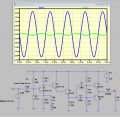
Oh you are right... Mine gives Zc = 36Ω >> 8 so I need a bigger cap. I tried 10 times 2200u lol, it works pretty well:
View attachment 323262
Try making RE3 = 2Ω (because SPICE circuits can't overheat your computer, although they would fry in real life) and you should be able to get it to work.
Then ask SPICE for the power dissipation in Q3 and RE3, and you'll see why it isn't normally done that way (although there are a few designers who do)
 

Thread Starter

babaliaris

Joined Nov 19, 2019
208
Try making RE3 = 2Ω (because SPICE circuits can't overheat your computer, although they would fry in real life) and you should be able to get it to work.
Then ask SPICE for the power dissipation in Q3 and RE3, and you'll see why it isn't normally done that way (although there are a few designers who do)
8ohm load design.png

Max of 2 Watts.

8ohm load design.png

Lol I destroyed it... haha

I need to buy some power transistors, you guys where correct. I don't have any though...

By the way, does the load actually get that power? Since it is coupled with the capacitor, no DC current goes though it, so how does it get the power?

It seems like the power is getting wasted in the Q3.
 

Jony130

Joined Feb 17, 2009
5,541
A sound amp between 20Hz-20kHz. Input (smartphone) impedance is unknown.
I see. Also in real-world design is necessary to have VEq1 > Vbe, for example, 1 in CE amplifier.
1d.PNG


I noticed that the Darlington amp does not work for 20Hz. Can it be improved?
But this is not the Darlington stage fault.
Notice that Cout together with RL form a high pass filter.
And you have set the low cutoff frequency to around Fc = 0.16/(RC) = 91Hz.
 

Attachments

Jony130

Joined Feb 17, 2009
5,541
Since it is coupled with the capacitor, no DC current goes though it, so how does it get the power?
But, the AC current is flowing through the load resistance. Thus, the power is also delivered to the load.

It seems like the power is getting wasted in the Q3.
This is normal for a class A amplifier. The power efficiency will be very pure less than 6%.
 

Ian0

Joined Aug 7, 2020
10,293
View attachment 323269

Max of 2 Watts.

View attachment 323271

Lol I destroyed it... haha

I need to buy some power transistors, you guys where correct. I don't have any though...

By the way, does the load actually get that power? Since it is coupled with the capacitor, no DC current goes though it, so how does it get the power?

It seems like the power is getting wasted in the Q3.
The efficiency peaks at 25% so you are sort-of-right - a lot of power is wasted in Q3.
You don't want DC current in a loudspeaker unless you want to fire the cone across the room. The capacitor (now that you have made it big enough) will let AC current flow in the speaker.

You could get 50% (in theory) if you replace RE3 with an inductor. A push=pull stage can manage 78.5%. If BC327/337 is all you have and you could dissipate 625mW in each, then you should (in theory) be able to put 4.5W into a speaker with a pushpull design. I hope you have plenty, because a few might go the way of all silicon before you get it right.
 

crutschow

Joined Mar 14, 2008
34,933
By the way, does the load actually get that power? Since it is coupled with the capacitor, no DC current goes though it, so how does it get the power?
You've never heard of AC power from a power line, (which generates no DC current)?

There is AC current going through the load, which generates power through a resistive load, that same as DC current would.
The power equals the square of the AC RMS voltage divided by the load resistance.
 
Top