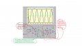
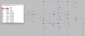
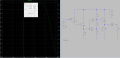
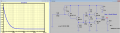
I can't figure out how to drive an 8Ω load!!!

Thread Starter

babaliaris

Joined Nov 19, 2019
208
You've never heard of AC power from a power line, (which generates no DC current)?

There is AC current going through the load, which generates power through a resistive load, that same as DC current would.
The power equals the square of the AC RMS voltage divided by the load resistance.
So, the 80mA current in Q3, what good does it do?

Does this stage exist only to drive the small 8Ω load, because the big 80mA current results in a small RE3 and an even smaller 1/gm3, so it achieves unity gain?
 

Ian0

Joined Aug 7, 2020
13,228
So, the 80mA current in Q3, what good does it do?
1/gm3, so it achieves unity gain?
None at all, but you can't avoid it.
RE3 must be low to be able to drive the negative half of the waveform. Even as low as 2Ω you have lost 20% of the voltage available to drive the speaker negative.
For the moment, assume that there is no capacitor, and that the speaker is connected to a voltage that is half the supply.
You can easily see that with Q3 not conducting what the maximum negative voltage across the speaker.
Does this stage exist only to drive the small 8Ω load, because the big 80mA current results in a small RE3 and an even smaller 1/gm3, so it achieves unity gain?
Q3 is an emitter follower. The maximum gain it can ever have is unity.
 

Jony130

Joined Feb 17, 2009
5,598
So, the 80mA current in Q3, what good does it do?

Does this stage exist only to drive the small 8Ω load, because the big 80mA current results in a small RE3 and an even smaller 1/gm3, so it achieves unity gain?
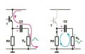
The problem is that the NPN transistor can only "source" the current and cannot "sink" current (current can only flow out of the emitter and never flow into the emitter). In your circuit, RE
resistor can only "sink" current.
Thus, the positive swing current is "provided" by BJT. But for the negative swing, we have a problem because now RE the resistor needs to be able to "sink" this negative current.

What this schematic is trying to show in a simplified manner:
6I6uc.jpg


Negative clipping occurs when IE current reaches IE=0A
(transistor is cut off).
Thus, the maximum negative voltage you can get at the output is equal to

Vout_max = V_EQ × RL/(RE+RL) = IEQ × RL||RE

Where:
V_EQ is a DC voltage at the Emitter

IEQ - Emitter quiescent current.

So to get a high output amplitude we need to have a high quiescent current.

In this example, you fed the Darlington output to a push-pull amp, and as a result, you got an even greater gain?
I lower the voltage gain. Because the signal from a smartphone will be "large".
And I add a push-pull to reduce the power dissipation across Q3. Thanks to this BD139 will survive without any additional external heatsink.
 

Thread Starter

babaliaris

Joined Nov 19, 2019
208
The problem is that the NPN transistor can only "source" the current and cannot "sink" current (current can only flow out of the emitter and never flow into the emitter). In your circuit, RE
resistor can only "sink" current.
Thus, the positive swing current is "provided" by BJT. But for the negative swing, we have a problem because now RE the resistor needs to be able to "sink" this negative current.

What this schematic is trying to show in a simplified manner:
View attachment 323274


Negative clipping occurs when IE current reaches IE=0A
(transistor is cut off).
Thus, the maximum negative voltage you can get at the output is equal to

Vout_max = V_EQ × RL/(RE+RL) = IEQ × RL||RE

Where:
V_EQ is a DC voltage at the Emitter

IEQ - Emitter quiescent current.

So to get a high output amplitude we need to have a high quiescent current.


I lower the voltage gain. Because the signal from a smartphone will be "large".
And I add a push-pull to reduce the power dissipation across Q3. Thanks to this BD139 will survive without any additional external heatsink.
I think this is the same with the way I understand it.

In an emitter follower configuration:

\[ A_{V} = V_{b_{in}} \frac {R_{E} // R_{L}}{\frac{1}{gm} + R_{E}//R_{L}} = V_{b_{in}} \frac {R_{E} // R_{L}}{\frac{V_{T}}{I_{C}} + R_{E}//R_{L}} \]

Now if the bias current:
\[ I_{C} \to \infty => \frac{V_{T}}{I_{C}} \to 0\]
so
\[ \frac {R_{E} // R_{L}}{ R_{E}//R_{L}} \to 1\]

So I'm almost achieving a unity gain.

This is why we need a big quiescent current and this is why I need this
configuration to get rid of the loading effect of the small RL.

Of course, I need to take into account the Rin trade-off, because:

\[ R_{in} \approx \frac{B}{g_{m}} + (b+1)[re + RE] =\frac{B}{g_{m}} + (b+1)[\frac{1}{g_{m}} + RE] \]

so:

\[ I_{C} \to \infty => g_{m} \to \infty => \frac{B}{g_{m}} \to 0, \frac{1}{g_{m}}\to 0 => Rin = (B+1)RE = Minimum Rin \]

And this is why I need another voltage buffer in between, with a big Rin and a Small Rout, so I can drive the small Rin from the emitter follower above.

And this is what the "middle" transistor in the Darlington configuration does. It achieves a big Rin, a relative 80-150Ω Rout which is << 800Ω of the resulting Power Amplifier Rin.

And because it is DC coupled, the base is at the same level as Vc1 = Vcc/2 = 10V, and at the same time I'm achieving a good DC offset to make sure my amplified signal won't drive the next two transistors to cut off at the negative swing. While the third transistor is going to have a DC base voltage of 10v - 0.7 = 9.3V which is still very high to make sure no clipping occurs!!!
 
Last edited:

Jony130

Joined Feb 17, 2009
5,598
Your equation for Rin is wrong. It cannot have β/gm and re at the same time. Because β/gm = r_pi and re = r_pi/(β + 1) or r_pi = (β + 1)*re
Also the load resistance seen by the first stage (CE amp) will be more than 100*100*(100Ω||8Ω) = 74kΩ (rin of a Darlington stage)
 

Ian0

Joined Aug 7, 2020
13,228
Just because the stage has a certain input resistance, you don't need to place a resistor of that value at the input!
And now is probably the time to introduce the concept of bias.
Examine what happens as you vary the voltage between the bases of Q4 and Q5.
 

Thread Starter

babaliaris

Joined Nov 19, 2019
208
Your equation for Rin is wrong. It cannot have β/gm and re at the same time. Because β/gm = r_pi and re = r_pi/(β + 1) or r_pi = (β + 1)*re
Also the load resistance seen by the first stage (CE amp) will be more than 100*100*(100Ω||8Ω) = 74kΩ (rin of a Darlington stage)
You are right, I confused that with the intrinsic Rout of an emitter follower which is 1/gm.
 

Jony130

Joined Feb 17, 2009
5,598
I set the voltage gain of a CE stage to be around 20V/V which should be enough for the signal levels from a smartphone.
And you are right about the need for a Darlington stage due to push-pull stage low rin. But there are better ways to drive push-pull stage, the more efficient way, directly from the CE stage. For example, by using the Darlington push-pull stage.

And R4 resistor does not set the Rin of a PP stage. His job is to remove the "dead zone". Take look here:
https://forum.allaboutcircuits.com/...ed-on-push-pull-amplifier.101749/#post-766570

And C1 and C2 short out this resistor for AC signal point of view. Thus rin becomes equal to R3||R4||(β + 1)*RL.
 

Thread Starter

babaliaris

Joined Nov 19, 2019
208
I set the voltage gain of a CE stage to be around 20V/V which should be enough for the signal levels from a smartphone.
And you are right about the need for a Darlington stage due to push-pull stage low rin. But there are better ways to drive push-pull stage, the more efficient way, directly from the CE stage. For example, by using the Darlington push-pull stage.

And R4 resistor does not set the Rin of a PP stage. His job is to remove the "dead zone". Take look here:
https://forum.allaboutcircuits.com/...ed-on-push-pull-amplifier.101749/#post-766570

And C1 and C2 short out this resistor for AC signal point of view. Thus rin becomes equal to R3||R4||(β + 1)*RL.
Thanks for the detailed explanation!!!

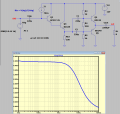
One more think before we conclude this thread. It seems I have a hard time figuring out how to measure Rin, Rout in LTspice, although I've already read a book about that..

The following results in a Rin=9.68Ω, which seems wrong. What Am I doing wrong?

Screenshot 2024-05-27 225302.png
 
Last edited:

Ian0

Joined Aug 7, 2020
13,228
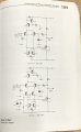
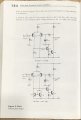
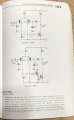
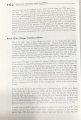
in order to drive an 8Ω load, I’d start from the differential amplifier that you were discussing previously. Here is a few pages from Linsley-Hood on the topic.
D84243F2-CD18-46C2-A8E9-04F2425B426E.jpeg7B4E2B6F-56D1-46E4-ADE6-23DE6FDEEC41.jpegE933C6B6-C33B-408F-8337-64D513A03D37.jpegFB6815ED-9B91-4708-A49A-F5A2CDC0583D.jpeg
 
Top