How this nanoampmeter works

Thread Starter

po210

Joined Dec 24, 2013
27
Hello
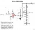
I found this circuit in LT1012 application notes pdf, and i cant understand how it works.
In usual trans impedance amplifier where current to be measured goes through negative input resistor, the op amp is trying to have zero volt different between its inputs, so it uses a feedback path to satisfy that making its output going negative. But here, i see a capacitor in the feedback, and a transistor that makes something similar.Why a transistor there?
Also, are Q1/Q2 here some kind of current mirror?. What role Q4 has? Adding +0.6V to op amp output? I see LT1004 fixes 1.2V for the different scales measuring resistors, but is confusing that adding Vbe decrements for Q3/Q2/Q4 path I get 1.8 at least..(unless Q4 goes off at some point)
What a mess for a poor hobbist like me...o_OCould somebody help please?
 

Attachments

Yffig

Joined Aug 25, 2019
34
I guess that the circuit works as a log-antilog amp according to the way Q1 is connected. The use of a CA3146 BJT array provides matched BJTs and temperature compensation. As the LT1012 model is included in LT-Spice and the use of 4 identical BJTs kinda 2N3904 should allow you to run a perfect LT-Spice simulation. Try it and you'll understand
 

michael8

Joined Jan 11, 2015
472
to a first approximation you can consider the opamp negative input network of 10K resistors as 0 ohms and the capacitor as open as there isn't an opamp DC path there . As you said, opamp inputs should be driven to be the same voltage (and one is grounded = 0V). So the other will be driven there too via path through Q1. Higher opamp negative input values will lower the opamp output pulling down the emitter of Q1 making it take more current from the opamp negative input...
 

WBahn

Joined Mar 31, 2012
32,824
1693622332915.png

Let's look at it in pieces. First, the LT1004C is a bandgap voltage reference that maintains 1.235V across it.

Now let's assume that R1 is at midrange, so call it 1000 Ω. That means that the total resistance in the emitter path of Q3 is nominally about 5560 Ω. Assuming a Vbe of about 650 mV for Q3, that means that the emitter current of Q3 is about Ignoring, for the moment, the Vce drop of Q3, that means the current is about 105 µA, making the voltage drop across each of the 549 Ω resistors about 58 mV.

This number is very significant, because, at room temperature, the collector current of a silicon diode (in the linear region) increases by an order of magnitude for every increase of ~59 mV in the base-emitter voltage. So this is key to understanding the operation.

Now let's consider the role of the input circuit at DC. The opamp will try to keep the input node at 0 V, since no current will be flowing in the capacitor or either of the 10 kΩ resistors at DC. To do that, the output of the opamp will go negative by a sufficient amount to create a Vbe on Q1 that corresponds to the input current. At the max input current of 100 µA, Q1 and Q2 will both have collector currents of 100 µA and the emitters of the transistors will be at about -650 mV. This current will then be flowing through the 33 kΩ resistor and sunk by the opamp. The voltage at the opamp output will therefore be about -7.25 V.

Q1 and Q2 effectively form a current mirror. Because the input node is held at 0 V, Q1 is effectively a diode-connected transistor. The base of the two transistors are virtually connected together. In the 100 µA range they ARE connected together, so Q2 will reflect the current in Q1, making it pull 100 µA to the meter when the input current is 100 µA. When the range switch is moved up to the 10 µA setting, the base voltage of Q2 is moved by enough to increase the collector current in Q2 by an order of magnitude, which results in it pulling 100 µA from the meter when the input current is just 10 µA.

I'm not sure what the intended roll of Q4 is. Under normal operation it's Vbe is about -650 mV, so it should be firmly in cutoff. My guess is that it is there to clamp the emitter voltages of Q1 and Q2 in the event of the current being applied in the wrong direction. I'm also guessing that the role of Q3 is to provide a degree of temperature compensation to the range offset string.
 

Yffig

Joined Aug 25, 2019
34
I made a LT-Spice simulation of the circuit... (see attached files).
Indeed Q1 and U1 are a log amp, providing an image of the natural log of I(input): see the voltage V(log) at the emitter of Q1. Q2 is the antilog feature: Ic (Q2)= K*exp (V(log)/Vth). As V(log) is always negative the diode connected BJT Q4 is reversed polarized and its current is only the leakage current Is which is very temperature sensitive providing temp compensation for the others BJT Q1 & Q2 which have the same Is as part of the same chip.
C1 offers a integrator feature to U1to limit the bandwith as the circuit is a DC amp-meter. The simulation running time is set very long for good operation of the integrator.
As shown by the simulations, the circuit, as it was published by Linear Tech, works very well at 100µA range, at 100nA the scale factor should be corrected (Radj to be set to 1.3k) & at 100pA, the scale factor and the linearity are not that good.
 

Attachments

Last edited:

Yffig

Joined Aug 25, 2019
34
Edit for LT-Spice simulation:
Investigating further I noticed that the current through R2 (that charges the 0.1µ integrator) causes the bad behaviour at low currents... I made a simulation for inputs currents 0 to 100pA without the integrator cap: the simulation shows then a very good behaviour ( the bias current from the LT1012 is only a few femto-amp...to good to be the real LT1012 ?).
This is really a very good idea to use a log-antilog feature to have that huge 6 decades of measurements. I thought that the LT1012 was a BiFet OpAmp...no it's a BJT one with input bias current compensation...well done LT-boys !
Sim 100pA without integrator.png
 
Last edited:

Yffig

Joined Aug 25, 2019
34
View attachment 301849

Let's look at it in pieces. First, the LT1004C is a bandgap voltage reference that maintains 1.235V across it.

Now let's assume that R1 is at midrange, so call it 1000 Ω. That means that the total resistance in the emitter path of Q3 is nominally about 5560 Ω. Assuming a Vbe of about 650 mV for Q3, that means that the emitter current of Q3 is about Ignoring, for the moment, the Vce drop of Q3, that means the current is about 105 µA, making the voltage drop across each of the 549 Ω resistors about 58 mV.

This number is very significant, because, at room temperature, the collector current of a silicon diode (in the linear region) increases by an order of magnitude for every increase of ~59 mV in the base-emitter voltage. So this is key to understanding the operation.

Now let's consider the role of the input circuit at DC. The opamp will try to keep the input node at 0 V, since no current will be flowing in the capacitor or either of the 10 kΩ resistors at DC. To do that, the output of the opamp will go negative by a sufficient amount to create a Vbe on Q1 that corresponds to the input current. At the max input current of 100 µA, Q1 and Q2 will both have collector currents of 100 µA and the emitters of the transistors will be at about -650 mV. This current will then be flowing through the 33 kΩ resistor and sunk by the opamp. The voltage at the opamp output will therefore be about -7.25 V.

Q1 and Q2 effectively form a current mirror. Because the input node is held at 0 V, Q1 is effectively a diode-connected transistor. The base of the two transistors are virtually connected together. In the 100 µA range they ARE connected together, so Q2 will reflect the current in Q1, making it pull 100 µA to the meter when the input current is 100 µA. When the range switch is moved up to the 10 µA setting, the base voltage of Q2 is moved by enough to increase the collector current in Q2 by an order of magnitude, which results in it pulling 100 µA from the meter when the input current is just 10 µA.

I'm not sure what the intended roll of Q4 is. Under normal operation it's Vbe is about -650 mV, so it should be firmly in cutoff. My guess is that it is there to clamp the emitter voltages of Q1 and Q2 in the event of the current being applied in the wrong direction. I'm also guessing that the role of Q3 is to provide a degree of temperature compensation to the range offset string.
In your analysis you state that Q1 & Q2 form a current mirror... that's wrong as your are forgetting the current sinked by the 33k resistor which is actually the difference between Ie(Q2) and Ie(Q1) and can be very high compared to Ie(Q1). The device is actually a log antilog amp.
 

WBahn

Joined Mar 31, 2012
32,824
In your analysis you state that Q1 & Q2 form a current mirror... that's wrong as your are forgetting the current sinked by the 33k resistor which is actually the difference between Ie(Q2) and Ie(Q1) and can be very high compared to Ie(Q1). The device is actually a log antilog amp.
The current sunk by by the 33 kΩ resistor is immaterial -- it's purpose is to hold the emitters of Q1 and Q2 at whatever Vbe corresponds to the current in Q1. The current in Q2 has no effect on that, merely on how far the opamp output has to go negative in order to make that happen.
 

Yffig

Joined Aug 25, 2019
34
The current sunk by by the 33 kΩ resistor is immaterial -- it's purpose is to hold the emitters of Q1 and Q2 at whatever Vbe corresponds to the current in Q1. The current in Q2 has no effect on that, merely on how far the opamp output has to go negative in order to make that happen.
Nobody has ever seen an "immaterial" current within Kirchoff's law. At Q1 & Q2 emitter junction, Kirchoff's law gives the algebric sum Ie(Q1) + Ie(Q2) + I(33k) + Is =0 .
Assuming Is is <<, the equation is simplified to Ie(Q1) + Ie(Q2) + I(33k) # 0.
Note that, whatever the range selected, Ie(Q2) drives a 100µA galvanometer which needs quite a few 10th µA to be easily readable. Therefore I(33k) is the complementary current needed to go from Ie(Q1) = I(input) to much more current (except for the 100µA range): it's in no way "immaterial". The Op Amp provides the necessary negative voltage from its output to the emitters via 33k to up to 100µA.
If you were to name the circuit, according to Wikipedia, The Art of Electronics.. among many others authors, this is not a "current mirror"(*). Instead, it's simply a current amplifier: Ic(Q2) = K* I(input), K being any power of 10 according to the selected range (e.g. for the 100 pA range, K is equal to 10^6, and for the 10 µA range K is 10, the circuit dynamic range is really impressive).
note(*): generally speaking, a current mirror reflects the input current with a unity gain, but some implementations provide small multiplier scalar coefficent (as far as I know this property is based on the area ratio of the active components utilized for that current mirror).
 

Yffig

Joined Aug 25, 2019
34
One more simulation in calibrating (1uA) mode:
View attachment 301909
Nice idea to have plotted the ratio beetwen I(Q2) and I(in) that shows the complementary effect of I(R3 ). Is the 10p compensation capacitor needed (the LT1012 is internally compensated for unity gain) ? Which simulation platform are you using ? (I run LTSpice 17.1.10 under Window 11).
 

Danko

Joined Nov 22, 2017
2,168
Nice idea to have plotted the ratio beetwen I(Q2) and I(in) that shows the complementary effect of I(R3 ). Is the 10p compensation capacitor needed (the LT1012 is internally compensated for unity gain) ? Which simulation platform are you using ? (I run LTSpice 17.1.10 under Window 11).
LTspice 17.0.37.0 under Windows 11 is used.
Without capacitor op-amp is oscillating, as it should be in real life:

1693679301416.png
ADDED:
In your analysis you state that Q1 & Q2 form a current mirror... that's wrong as your are forgetting the current sinked by the 33k resistor which is actually the difference between Ie(Q2) and Ie(Q1) and can be very high compared to Ie(Q1).
Nice idea to have plotted the ratio beetwen I(Q2) and I(in) that shows the complementary effect of I(R3 ).
Seems 33k resistor is not guilty.
See simulation:
1693707474747.png___1693707697420.png
 

Attachments

Last edited:

WBahn

Joined Mar 31, 2012
32,824
Nobody has ever seen an "immaterial" current within Kirchoff's law. At Q1 & Q2 emitter junction, Kirchoff's law gives the algebric sum Ie(Q1) + Ie(Q2) + I(33k) + Is =0 .
Assuming Is is <<, the equation is simplified to Ie(Q1) + Ie(Q2) + I(33k) # 0.
Note that, whatever the range selected, Ie(Q2) drives a 100µA galvanometer which needs quite a few 10th µA to be easily readable. Therefore I(33k) is the complementary current needed to go from Ie(Q1) = I(input) to much more current (except for the 100µA range): it's in no way "immaterial". The Op Amp provides the necessary negative voltage from its output to the emitters via 33k to up to 100µA.
If you were to name the circuit, according to Wikipedia, The Art of Electronics.. among many others authors, this is not a "current mirror"(*). Instead, it's simply a current amplifier: Ic(Q2) = K* I(input), K being any power of 10 according to the selected range (e.g. for the 100 pA range, K is equal to 10^6, and for the 10 µA range K is 10, the circuit dynamic range is really impressive).
note(*): generally speaking, a current mirror reflects the input current with a unity gain, but some implementations provide small multiplier scalar coefficent (as far as I know this property is based on the area ratio of the active components utilized for that current mirror).
Note that I said, in my first post, that Q1 and Q2 "effectively" form a current mirror.

How does a basic current mirror work? A current is forced through a diode-connected transistor. The resulting Vbe of that transistor is then applied to a second transistor. If that transistor is adequately matched and has sufficiently high output resistance, that Vbe produces the same collector current in the second transistor as in the first.

That is EXACTLY how Q1 and Q2 behave when the range select is set to the 100 µA range. I walked through how and why it behaves this way in detail. With the range setting in other than the 100 µA range, the Vbe offset results in the scaling effect in the same manner that a Widlar current mirror does, except instead of using a resistor in the input transistor's emitter leg to produce a ~60mV/decade rise in the output transistor's Vbe, this circuit uses the resistor divider chain to do the exact same thing.

I also explained, quantitatively, how the range select functionality behaves. All you've said is that, somehow, the range select results in K being some power of ten corresponding to each range, but you haven't given any indication of why or how. Yet, treating Q1 and Q2 as forming an effective current mirror, I was able to explain exactly how those specific values of K come about as a direct consequence of the specific component values on the right side of the circuit.
 

Yffig

Joined Aug 25, 2019
34
Note that I said, in my first post, that Q1 and Q2 "effectively" form a current mirror.

How does a basic current mirror work? A current is forced through a diode-connected transistor. The resulting Vbe of that transistor is then applied to a second transistor. If that transistor is adequately matched and has sufficiently high output resistance, that Vbe produces the same collector current in the second transistor as in the first.

That is EXACTLY how Q1 and Q2 behave when the range select is set to the 100 µA range. I walked through how and why it behaves this way in detail. With the range setting in other than the 100 µA range, the Vbe offset results in the scaling effect in the same manner that a Widlar current mirror does, except instead of using a resistor in the input transistor's emitter leg to produce a ~60mV/decade rise in the output transistor's Vbe, this circuit uses the resistor divider chain to do the exact same thing.

I also explained, quantitatively, how the range select functionality behaves. All you've said is that, somehow, the range select results in K being some power of ten corresponding to each range, but you haven't given any indication of why or how. Yet, treating Q1 and Q2 as forming an effective current mirror, I was able to explain exactly how those specific values of K come about as a direct consequence of the specific component values on the right side of the circuit.
It is easy to obtain the gain K of the current amplifier which I described as a log-antilog device:
Assuming that all currents are >> Is, all BJTs are identical, and all Ic=Ie, one can write:
I(in)=Ic(Q1)=Ie(Q1)= Is*exp[Vbe(Q1)/Vth] (Vth = kT/q about 26 mV at room temperature, small k is Boltzman's constant)
gives Vbe(Q1)= Vth*ln(Iin/Is) (this is the log part of the circuit)
For Q2: Ic(Q2)= Is*exp[Vbe(Q2)/Vth] (this is the "anti-log" part of the circuit)
Let's call the potential at the base of Q2: Vx
Vbe(Q2)= Vx-(-Vbe(Q1))=Vx+Vbe(Q1)
hence Ic(Q2)= Is*exp[(Vx+Vbe(Q1))/Vth] =
Ic(Q2)=[Is*exp(Vbe(Q1)/Vth)]*[exp(Vx/Vth)]
The first term of the product is simply I(in), the second one is K, the current amplification factor

The operation of the circuit is therefore:
Ic(Q2)= K*I(in) with K = exp(Vx/Vth)
For a given K, the value of the necessary Q2_base potential (Vx) is therefore: Vx=Vth*ln(K).......that's all folks !

For K=10, given Vth at room temp = 26 mV, Vx=26mV*ln(10)=26mV*2.30=59.87mV
For K=100, given Vth at room temp = 26 mV, Vx=26mV*ln(100)=26mV*4.60=119.73mV etc....

This formula also allows to select any value of K as needed.
But notice that the current amplification factor K is highly sensitive to the temperature as Vth = kT/q. Hence the ratio Vx/Vth should remain constant whatever T is : this the role played in a certain way by the diode connected BJT Q3
 

Thread Starter

po210

Joined Dec 24, 2013
27
I've been following the thread and honestly, i can only give both of you many thanks not only for the high level of your explanations, but also for taking the effort to simulate this circuit.
Although I've known for years about the exponential dependency Ic ~ Vbe in bipolar transistors, I think is the first time I see a direct application of this dependency besides the typical uses in ( linear) amplification.I was trying to figure out what was the reason for those ugly values for resistor and now is clear.

To be honest, I cant see much controversy in your both interpetations. When i though in "current mirror" i was thinking more in two transistor with joined bases forced to sink the same current in the operational amplifier than in a fully fledged mirror. If i understood properly, now i see there is a K factor in the current, so is not exactly a mirror...but for me the problem was more in understanding the role of resistors at circuit righ side, and both of you explained the "exponential reason" of that.
My hat off!

As always, noise will ruin my effort but...I have ordered an AS3046.
 

Yffig

Joined Aug 25, 2019
34
I've been following the thread and honestly, i can only give both of you many thanks not only for the high level of your explanations, but also for taking the effort to simulate this circuit.
Although I've known for years about the exponential dependency Ic ~ Vbe in bipolar transistors, I think is the first time I see a direct application of this dependency besides the typical uses in ( linear) amplification.I was trying to figure out what was the reason for those ugly values for resistor and now is clear.

To be honest, I cant see much controversy in your both interpetations. When i though in "current mirror" i was thinking more in two transistor with joined bases forced to sink the same current in the operational amplifier than in a fully fledged mirror. If i understood properly, now i see there is a K factor in the current, so is not exactly a mirror...but for me the problem was more in understanding the role of resistors at circuit righ side, and both of you explained the "exponential reason" of that.
My hat off!

As always, noise will ruin my effort but...I have ordered an AS3046.
The "ugly" resistors voltage divisor (with a good temp compensation) will allow you to choose the full scale current you desire.
If you're interested, I made a LT-Spice simulation with temp from 15°C to 35°C (or whatever temp range you'd like).
Let me know.
By the way the difference between CA3046 and CA3146 is that the 3146 will withstand much higher voltage (30V vs 15V max) but with a power supply of +/- 12V that should run OK.
 
Last edited:

WBahn

Joined Mar 31, 2012
32,824
I've been following the thread and honestly, i can only give both of you many thanks not only for the high level of your explanations, but also for taking the effort to simulate this circuit.
Although I've known for years about the exponential dependency Ic ~ Vbe in bipolar transistors, I think is the first time I see a direct application of this dependency besides the typical uses in ( linear) amplification.I was trying to figure out what was the reason for those ugly values for resistor and now is clear.

To be honest, I cant see much controversy in your both interpetations. When i though in "current mirror" i was thinking more in two transistor with joined bases forced to sink the same current in the operational amplifier than in a fully fledged mirror. If i understood properly, now i see there is a K factor in the current, so is not exactly a mirror...but for me the problem was more in understanding the role of resistors at circuit righ side, and both of you explained the "exponential reason" of that.
My hat off!

As always, noise will ruin my effort but...I have ordered an AS3046.
Both interpretations are valid. As is often the case, there are multiple ways to analyze/design a circuit.
 

Yffig

Joined Aug 25, 2019
34
I choose 1% resistors with a (medium) tempco of 50ppm and run the simulations for 0...1µA input at 3 temperatures: 25°C, 15°C and 35°C.
At 25°C : I peaks at 100.2µA
At 15°C : I peaks at 101.84µA
At 35°C : I peaks at 98.64µA
that is less than 2% for a 10°C change. For me it's OK for an analog equipment.
1µA with temp.png
 

Attachments

Yffig

Joined Aug 25, 2019
34
I made a huge improvement to the temp behaviour of the circuit by using a LM334 which a current source linearly dependent of temp. The LM334 is set at about 100µA by the resistor R4.
The idea is very simple... : as demonstrated earlier, the current gain coefficient is K = exp (Vx*q/kT), so the circuit is highly dependent of the ambiant temperature T (Kelvin). If Vx is made linearly dependent of T (that is Vx=α.T) then K = exp (α.T.q/k.T) = exp (α.q/k) is independent of the temperature.
The variation of I(100µA) from 15° to 35° is only 0.21µA which is about 20 times less than that of the original circuit !
The LM334 drives a resistor calculated for generating the desired Vx.
The LT1004 is no longer needed.... the LM 334 is almost insensitive to small variations of the power supply +15V
Below is the simulation on the 1µA range from 0° to 50°C. Attached are also the .asc, .asy and .sub files if needed.

1µA temp compensated with LM334.png.
 

Attachments

Last edited:
Top