for me this is crystal clear. i have used various SMPS for years. and buck converters are very straight forward.
also every simulator will have some examples - likely using different IC but... the principle is the same. one just need to keep track of few things..
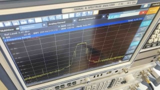
for example if you feel like probing around and checking waveforms, knock yourself out:
but that was variant 17555A with 3.3V reference so no voltage divider on output. but there is variant C, whcih uses 0.8V feedback.
this one is closer match to IC you chose wanted - the noticeable difference is that this one has built in diode and some other inputs like reset and hysteresis:
it has larger value inductor and can handle different load range but if you want to see how it works, this is close enough.
and since reference voltage is the same (0.8V), using same resistor value for feedback voltage divider gets you same same output voltage 3.3V:
this gives you taste of what happens when you change something. which is what simulators are good for (test drive things without blowing parts). see what the trends are... like when adjusting voltage divider (which is in most cases the ONLY thing you may want to adjust anyway). simulators are neat but will happily lie to you too (they are not 100% accurate). which is why ultimate test is test on the real hardware. but they are great to explore things. for example try the last circuit and see how things change if you use different value for C2.... try different values in range like 1uF to 50uF.
i hope this helps and you need to make your own choices.
if you have a reference design and example how to calculate things, i don't see need for much experimenting.
if you are not certain, build it. make a small board and test it.
NO!!! I mean verifying that the PCB artwork is all accurate. The entire circuit would be engineered and verified before the PCB design begins. The time for failures is when the design is still on paper. NOT after a production run of product is built.
 Facebook
 Google
 GitHub
 Linkedin