Hold push button, timer, then activate relay.

crutschow

Joined Mar 14, 2008
34,280
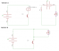
Due to a glitch in the generation of the Clk signal I observed in my simulations of a similar circuit, I have modified the circuit by adding D3 and R5 to generate some positive feedback hysteresis to FF U2 (used as a NI buffer) as shown below.

upload_2017-1-4_12-4-22.png
 

Attachments

Last edited:

syshex

Joined Dec 27, 2017
10
Hi there ! First of all, I'm just starting ( the past 6 months ) learning about electronics so this is all quite new to me, and a bit hard to follow.

Looking at the circuit I'm having a real hard time to understand how this does what it does. (I have not built or tested it )

I have a few questions if you don't mind.
- Q in U1 and Q- in U2 are connected to what? Are they left unconnected?
- While not powering the relay , when the circuit is in the Off state , does it have any consumption? I see paths from + to - of the V1 battery are achieved only through the CD4013B unit and trough the relay itself if the Q1 transistor allow it, or through the switch if it is closed.

On the practical side, I was looking for a circuit like this to provide on and off functionality for an atmega micro . I'm wondering what would be the best way to go about this. I'm thinging of two possibilities:

1- Replace the relay with a component that works like the relay, by being a switch and have this circuit power that switch. The battery would also be connected to the second circuit .

2- Get the power for the operation of the second circuit (with the atmega) directly from the first circuit, using the + and - to operate the relay as source for the second circuit.

Now, I probably am not making much sense and these ideas might be rubbish, so could I get some comments and possible direction for me to take? I'm used to software development, but electronics is a complete new ballpark for me.

Thanks so much for your time!

MOD:
@crutschow
 

Tonyr1084

Joined Sep 24, 2015
7,852
Welcome to AAC.

The 4013's are but a single package. You might know it's called a "Dual D Flip Flop". The power going directly to the CLR is just the Clear connection. It must be held high in order for the chip to function. The "Q" and the "Q with a bar over it" are called "Q" and "NOT Q". At all times (with one rare exception) one is always in the opposite state of the other. In other words when Q is high (powered on) NOT Q is low (connected to ground). (And there's been much debate over calling it ground or common, but we won't get into that). The Flip Flop (FF) only uses power when it changes state. Well, not 100% true, but pretty much doesn't use power when not changing states. The CLK (Clock) input is where the FF gets the command to change state. On the second FF you see NOT Q connected to D (Data) and Q is connected to nothing. It's output is not needed in this circuit. NOT Q is also connected to the base leg of the 2N2222 transistor, a common general purpose low power device which only turns on when there is a small current on its base. When NOT Q is at zero (Low) volts there is no current to the 2222. That keeps the transistor from turning on. When NOT Q goes high (turns on) current flows through the current limiting resistor and turns the 2222 on, which provides ground (common, return, negative) for the relay. The 2222 IS a switch in this circuit. The purpose here is to control the relay which draws very little current. The relay can switch much higher currents and can switch voltages that are not the same as the circuit controlling the relay.

Recommendations for future posts: Where you find the general questions you'll also find a "Post new thread" or something like that. Click that button and start your own question. The guys here are very helpful and able to explain much more than I can about a great deal more of electrical and electronic circuits. I just know some basics.

Enjoy your time here. Never be afraid to ask a question, even if you think it's a stupid one. The only truly stupid thing to do is to not ask and not learn.
 

syshex

Joined Dec 27, 2017
10
...... The 2222 IS a switch in this circuit.
Thank you so much Tonyr . After reading your comment, I went back to the diagram, and finally understood it in general. Yes the 2222 is a switch, it took your comment for it to click. The lack of experience in electronics can be very frustrating... thanks so much.

Do you want to switch the supply power the atmega?
I really have no idea if that is the correct way to go about it. It is one of the solutions that I though about. The other being the Battery powering both circuits (this one and the one I designed ) and have a relay of sorts (like the one on this diagram) to turn on and off the other circuit.

My battery is going to be a 3.7V 190MAH LiPO or 3.7 V 1100 mAh (yes I know, one is almost 10x the capacity of the other ) . I have a circuit that I designed, based of the https://learn.adafruit.com/adafruit-feather-32u4-basic-proto/downloads , and two other sensors together.

I'm sorry for my English if I didn't explain myself correctly and didn't use the correct terminologies.
 

syshex

Joined Dec 27, 2017
10
You said:
So how are you thinking about doing this?
Do you just want to turn the operation of the atmega on and off with the power continually on, or do you want to remove the power from the atmega?
Hi! Thanks so much for taking the time. I uploaded the two versions I had in mind. In both versions, a simplified version of your circuit is on the left .

In version 1 , the circuit on the right and the circuit on the left are connected to the same V1 battery. when you circuit closes the relay , the K1 relay closes the circuit on the right.

In Version 2 , I remove the relay and place my circuit in that place.

My doubts with regards to version 2, is if the 2222 will handle the power that will be drained for the atmega and my two sensors well.
 

Attachments

crutschow

Joined Mar 14, 2008
34,280
if the 2222 will handle the power that will be drained for the atmega and my two sensors well.
Likely, but we need to know how much total current they require to answer that question.
If you don't know the answer, then you could just use a power MOSFET for the switch which will likely handle and current they are likely to take.
 

syshex

Joined Dec 27, 2017
10
Likely, but we need to know how much total current they require to answer that question.
If you don't know the answer, then you could just use a power MOSFET for the switch which will likely handle and current they are likely to take.
Thanks so much for this help. I'll check the current drain of each of the components in their datasheets and compare with values allowed for the 2222. If it exceeds , I'll give a look at replacing the 2222 with a power MOSFET.

Thanks so much once again
 

syshex

Joined Dec 27, 2017
10
Hello again.

I was looking at the CD4013B component (http://www.ti.com/lit/ds/symlink/cd4013b.pdf) , and I'm selecting the CD4013BM package .
Looking at the pinout I see the VDD and VSS pins , that are not shown on the diagram. Not too sure what to do with those, since I'm not wanting to have the VDD connected to the power supply directly as it would be draining the battery even when the button is not pressed and the circuit is not on the On state.

Can anyone give me a hand?

So sorry about this!
 

crutschow

Joined Mar 14, 2008
34,280
Looking at the pinout I see the VDD and VSS pins , that are not shown on the diagram. Not too sure what to do with those, since I'm not wanting to have the VDD connected to the power supply directly as it would be draining the battery even when the button is not pressed and the circuit is not on the On state.
Yes, power and ground are often not shown on a digital circuit schematic but the connection is implied.
Vdd is connected to power and Vss connected to ground.

It will not drain the battery significantly since a CMOS logic circuit only draws a very small leakage current when static. Even a coin cell will power them for years.
Look at the data sheet.
 
Top