 Facebook
 Google
 GitHub
 Linkedin
Hi,
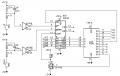
The CD40192 specifies minimum pulse widths for the various inputs. It also lists some propagation delays from this input to that output but only maximum and typical values, no minima.
Given the attached circuit, when the CD4028 counts down from S0 to S9, with a very short propagation delay is there the possibility of some kind of race condition? S9 will trigger load on the CD40192 which will program S9 low thereby short-cutting the pulse width on the load input to below minimum specification?
Or, S9 goes low and thus the load has obviously already occurred then there can never be a race condition? The same reasoning may be applied to S4 -> MR.
Attachments
-
 45.9 KB Views: 21
 -
88 KB Views: 4


