Hold push button, timer, then activate relay.

Thread Starter

IntempoDK

Joined Dec 29, 2016
9
It won't work. You have the timer configured as a one shot that will trigger as soon as the button is pressed. That will toggle the flip flop as soon as the button is pressed.

You have to let the timer time out and add some logic to implement your 5 second button hold requirement. Once you do that, you'll have more components than the last solution offered.
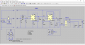
Can you write me a list of what to purchase for it?
Half of the items on his diagram im not even sure what is :D

If possible, even a diagram like the one i made, its ALOT easier for me to find round in that.
 

Attachments

crutschow

Joined Mar 14, 2008
34,281
but the simpler the better in this case, i have to be able to make it too

If i can do it without the 4027B then its even better, if any can look at this and tell me if its going to work or not
It won't work as shown, as dl324 noted.

You need a toggle flip-flop, such as the 4013, for you circuit.
A flip-flop latch, such as a 555 configured for that, won't readily do what you want.

As far as simple, the circuit I posted in post#15 has fewer parts than yours (requiring only one IC).
You can substitute a BJT (bipolar transistor) for the MOSFET to drive the relay if you like, as shown here.
upload_2016-12-30_8-52-57.png
 

Attachments

Last edited:

Thread Starter

IntempoDK

Joined Dec 29, 2016
9
It won't work as shown, as dl324 noted.

You need a toggle flip-flop, such as the 4013, for you circuit.
A flip-flop latch, such as a 555 configured for that, won't readily do what you want.

As far as simple, the circuit I posted in post#15 has fewer parts than yours (requiring only one IC).
You can substitute a BJT (bipolar transistor) for the MOSFET to drive the relay if you like as shown here.
View attachment 117752
Thanks, but im having a bit of a bind finding around in our diagram, im used to the ones like i posted, looks like you have a simulation cirquit, and where does push button come in? the hold relay where i attach the inverter and so on, maybe a diagram a bit like the one i made below, that one i can read :D ?
 

Attachments

crutschow

Joined Mar 14, 2008
34,281
Thanks, but im having a bit of a bind finding around in our diagram, im used to the ones like i posted, looks like you have a simulation cirquit, and where does push button come in? the hold relay where i attach the inverter and so on
I simplified the circuit by removing the simulation stuff, so it should be easier to understand.
You can get the pinouts for the CD4013, including power and ground, from its data sheet here.
The two flip-flops shown (U1 and U2) are actually in one CD4013 package.
SET is the same as PRE and CLEAR is the same as CLR.

I know reading schematics can be a little confusing to the newbie but after a little practice it should become easier.
Normally the signal flow is from left to right, with the power going from top to bottom.
The triangle symbol indicates circuit common.

Be sure and double-check the circuit after you build it.
Most circuit problems are due to wiring errors and/or using the wrong pinout for a part.
I use a highlighter pen to mark off each connection on the schematic as I do a continuity check on the circuit.

Any further questions you have on all this or if you need help with the parts, let us know.

upload_2016-12-30_9-34-50.png
 
Last edited:

Thread Starter

IntempoDK

Joined Dec 29, 2016
9
I simplified the circuit by removing the simulation stuff, so it should be easier to understand.
You can get the pinouts for the CD4013, including power and ground, from its data sheet here.
The two flip-flops shown (U1 and U2) are actually in one CD4013 package.
SET is the same as PRE and CLEAR is the same as CLR.

I know reading schematics can be a little confusing to the newbie but after a little practice it should become easier.
Normally the signal flow is from left to right, with the power going from top to bottom.
The triangle symbol indicates circuit common.

Be sure and double-check the circuit after you build it.
Most circuit problems are due to wiring errors and/or using the wrong pinout for a part.
I use a highlighter pen to mark off each connection on the schematic as I do a continuity check on the circuit.

Any further questions you have on all this or if you need help with the parts, let us know.

View attachment 117757
Thanks, this is greatly appreciated :)
I will order the components and see if it works out :)
 

Tonyr1084

Joined Sep 24, 2015
7,852
Crutschow: If you drive the preset high (U2) and it drives Q high, how are you resetting Q back to low? Does driving preset and reset high at the same time result in Q and /Q going high so that when preset goes low Q goes low again?
 

Thread Starter

IntempoDK

Joined Dec 29, 2016
9
I simplified the circuit by removing the simulation stuff, so it should be easier to understand.
You can get the pinouts for the CD4013, including power and ground, from its data sheet here.
The two flip-flops shown (U1 and U2) are actually in one CD4013 package.
SET is the same as PRE and CLEAR is the same as CLR.

I know reading schematics can be a little confusing to the newbie but after a little practice it should become easier.
Normally the signal flow is from left to right, with the power going from top to bottom.
The triangle symbol indicates circuit common.

Be sure and double-check the circuit after you build it.
Most circuit problems are due to wiring errors and/or using the wrong pinout for a part.
I use a highlighter pen to mark off each connection on the schematic as I do a continuity check on the circuit.

Any further questions you have on all this or if you need help with the parts, let us know.

View attachment 117757
The CD4013B, the only one i can find any my supplier here is `
Logik IC - Flip-Flop Texas Instruments CD4013BE Set (standart) and reset differential DIP-14
would that be okay?
And the Eletrocondensator, 22 uF special voltage? or 50Vs good enough?
 

Attachments

Jony130

Joined Feb 17, 2009
5,487
Crutschow: If you drive the preset high (U2) and it drives Q high, how are you resetting Q back to low? Does driving preset and reset high at the same time result in Q and /Q going high so that when preset goes low Q goes low again?
Yes, you are on the right track
http://forum.allaboutcircuits.com/threads/ltspice-and-cd4013.129753/#post-1065138
The CD4013B, the only one i can find any my supplier here is `
Logik IC - Flip-Flop Texas Instruments CD4013BE Set (standart) and reset differential DIP-14
would that be okay?
CD4013 from Texas Instruments is what you need.
And the Eletrocondensator, 22 uF special voltage? or 50Vs good enough?
Every capacitor with voltage rearing >> 5V (1.5 times Supply voltage) is good.
 
Last edited:

crutschow

Joined Mar 14, 2008
34,281
Here's a variant of crutschows circuit.
As I noted previously, the problem with such a circuit is that the 4013 has a clock maximum rise and fall time requirement, as the clip from the data sheet shows below.
upload_2016-12-30_19-0-37.png
Thus, although it may simulate okay, the slow RC clock risetime from the input delay circuitry could be problematic in the actual circuit.
This is one case where the simulation can give erroneous (good) results since the model likely doesn't include provisions for failure if the clock risetime is too slow that the actual circuit may exhibit.
 
Last edited:

eetech00

Joined Jun 8, 2013
3,858
As I noted previously, the problem with such a circuit is that the 4013 has a clock maximum rise and fall time requirement, as the clip from the data sheet shows below.
View attachment 117784
Thus, although it may simulate okay, the slow RC clock risetime from the input delay circuitry could be problematic in the actual circuit.
This is one case where the simulation can give erroneous (good) results since the model likely doesn't include provisions for failure if the clock risetime is too slow that the actual circuit may exhibit.
Good point....I'll have to rethink the input circuit..
 

eetech00

Joined Jun 8, 2013
3,858
Hi

Just reporting back that I bread boarded the circuit in post #32. I didn't drive a mosfet, but an LED connected from pin 2 to +5.

The circuit does work as intended. On power up, U2b Q bar is set high. When +5 is applied to the input, the LED lights up after about 5 seconds,
and shuts off when +5 is removed from the input.

As an additional test, I replaced the input circuit with a slow ramp using a function generator. Still operated as intended.

eT
 

crutschow

Joined Mar 14, 2008
34,281
As an additional test, I replaced the input circuit with a slow ramp using a function generator. Still operated as intended.
Then it is operating well outside its stated limits.
But, in general, it's not good practice to build a circuit that knowingly operates outside the devices specification limits. It could come back to bite you at a latter time (for example at a different operating voltage or temperature). :eek:
 

dl324

Joined Mar 30, 2015
16,845
in general, it's not good practice to build a circuit that knowingly operates outside the devices specification limits.
+1 for that. Manufacturers don't guarantee operation outside of their specs and parts from different lots/manufacturers may behave differently. (OP mentioned in post #16 that he wanted others to be able to build the circuit.)

Using a part outside of the guaranteed specs requires incoming testing for desired behavior. HP used to do it. It must have been more economical for them to do the screening themselves vs. paying the manufacturer for custom specs.
 

eetech00

Joined Jun 8, 2013
3,858
Then it is operating well outside its stated limits.
But, in general, it's not good practice to build a circuit that knowingly operates outside the devices specification limits. It could come back to bite you at a latter time (for example at a different operating voltage or temperature). :eek:
Understood...
 
Top