Facebook
 Google
 GitHub
 Linkedin
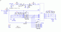
You cannot assume that when nothing is connected to the input of a gate that the logic input is 0.
Nothing is not 0.
This is a common mistake made by the uninitiated.
You must have a way to pull the input to logic LOW or logic HIGH.
When interfacing to non-CMOS logic such as 7400, 74LS00 series gates it is preferable to have the switch create a short to GND.
Use a 1k to 5kΩ pull-up to Vcc (+5V).
You must connect /1G and /2G of 74LS244 to the inverted signal of /OE of the SRAM otherwise the two circuits will be in contention.
What does this mean?
The 74LS244 and HM6116 devices both have output capability. You cannot have both in the output state at the same time. Only one device can be enabled as output.
74LS244 is a dual 4-bit bus driver. You do not need two chips unless you find it easier to layout the connections by using two chips.