HM6116A120 RAM Design writable addressable circuit

Thread Starter

Steven Diveley

Joined Dec 1, 2018
14
Merry Christmas and Happy Holidays everyone,

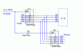
This week I am focusing on designing an Addressable RAM circuit, using the HM6116A120 SRAM chip. I think i got a pretty good understanding of the process so far. We are required to use the chip mentioned above, while building an addressable RAM circuit. We are to basically assign values to an address and call back upon the address to get the inverted results. For example A1 = 1001, output = 0110. The are I am stuck in is how to wire the address bus to make this work. Where I am at now, each bus seems to only take one binary value when they should be able to store much more. So im assuming the issue lies in how the address bus is wired. The chip uses bidirectional Data Busses which I am using to to assign these values via a DSWPK8 switch. Where i stand now, when assigning the values the results do appear to be read inverted, but they do not appear to be assigned to an address.

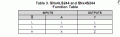
I am also using a DSWPK8 switch to give the address either a high or low, it was under my impression if the address had a high input the written data will be assigned to this address, which i could write to multiple addresses, then read the inverted binary value later. This does not seem to be the case, as the only results i have gotten are from the current written process and have not been able to read previous addressed written to. Here is what i have so far, ive also tried to use pull down resistors but they didnt seem to help and in some case prevented the simulation from occurring. Also information about the OE control bus would be helpful. I have found the OE cannot be high while WE is high, and cannot be low when WE is low. Screenshot 2018-12-23 10.24.42.png
 

ericgibbs

Joined Jan 29, 2010
21,439
hi Steven,
Have you downloaded a copy of the 6116 NRAM. d/s?
Check out the timing diagrams.
Also its a CMOS device, do not leave inputs disconnected.
E
 

Attachments

dl324

Joined Mar 30, 2015
18,326
Learn how to minimize wire crosses and jogs:
This:
upload_2018-12-23_8-28-40.png
can be drawn like this:
upload_2018-12-23_8-29-27.png
Note: I used the first 8 bit memory type device I found.
 

MrChips

Joined Oct 2, 2009
34,807
The SRAM data pins are bidirectional I/O lines.
You cannot hard-wire these to logic 0/1.
Use a tri-state bus drive to drive the lines 0/1 only when you want to write data to the SRAM.
 

Thread Starter

Steven Diveley

Joined Dec 1, 2018
14
hi Steven,
Have you downloaded a copy of the 6116 NRAM. d/s?
Check out the timing diagrams.
Also its a CMOS device, do not leave inputs disconnected.
E
I have looked over the datasheet, failed to understand the address bus. Does this mean I cannot go from one address straight to the next? With a 20 ns write time and a 120ns read time. As for do not leave inputs disconnected I am assuming you are referring to A8, A9, and A10. I will make the switch to a DPSKW4 and a DPSKW5 in order to correct this mistake.
 

Thread Starter

Steven Diveley

Joined Dec 1, 2018
14
The SRAM data pins are bidirectional I/O lines.
You cannot hard-wire these to logic 0/1.
Use a tri-state bus drive to drive the lines 0/1 only when you want to write data to the SRAM.
To implement a tri-state bus drive, the swithes will then be connected to the top pin, with the data in pin connected to the I/O and data out connected to the Probes? We havent covered tri-state buffers in 3 years so this is a little new to me.
 

ericgibbs

Joined Jan 29, 2010
21,439
hi,
The d/s I posted, Pages #7 and #9 show the Read and Write waveforms.
Chose either CS or WR version.
Are you able to create these waveforms, using switches.??
E
 

MrChips

Joined Oct 2, 2009
34,807
To implement a tri-state bus drive, the swithes will then be connected to the top pin, with the data in pin connected to the I/O and data out connected to the Probes? We havent covered tri-state buffers in 3 years so this is a little new to me.
Tri-state is not difficult to understand. Look up 74HC244 and 74HC245.
 

dl324

Joined Mar 30, 2015
18,326
Will correct this issue right now. It does look easier to read and see where everything is going.
Well drawn schematics are a form of art. You want to communicate circuit intent, so you want to avoid unnecessary distractions.

Learn how to use the shift key to get Multisim make straighter routes. When it refuses, let it do it's messy route and move the wire manually.
 

Thread Starter

Steven Diveley

Joined Dec 1, 2018
14
Tri-state is not difficult to understand. Look up 74HC244 and 74HC245.
I have connected two 74LS244N octal buffers and I seem to be getting the same results.I downloaded the data sheet for the pin references from Texas Instruments, and currently looking for a more descriptive D/S since TI doesnt inform me on what the 1G input does.
 

Thread Starter

Steven Diveley

Joined Dec 1, 2018
14
hi,
The d/s I posted, Pages #7 and #9 show the Read and Write waveforms.
Chose either CS or WR version.
Are you able to create these waveforms, using switches.??
E
I thought the purpose of the switches were to create the waveform needed. Such as CS = L, OE = L. WE = H to create the waveform needed to read the addresses. I honestly do not know.
 

ericgibbs

Joined Jan 29, 2010
21,439
hi,
I would suggest that you consider a WRITE push button with added logic, say a 555 timer that generates the Write 'pulse'.
Also the same method for a READ pulse.
The 1G LS244 is used to set the Buffers into ON state [ ie: output follows the input] when 1G is LOW.
When the 1G is HIGH the LS244 output pins are high Z, [ ie: open circuit]
Do you follow OK.
E
 

MrChips

Joined Oct 2, 2009
34,807
I have connected two 74LS244N octal buffers and I seem to be getting the same results.I downloaded the data sheet for the pin references from Texas Instruments, and currently looking for a more descriptive D/S since TI doesnt inform me on what the 1G input does.
Show a circuit diagram of how you connect your 74LS244.
You do not need two 74LS244. One will do for 8-bit bus.
Connect /1G and /2G together. The / over the signal name indicates that the signal is ACTIVE-LOW, i.e. it needs a LOW signal to activate the function.

You want to connect /1G and /2G to a signal that is a LOW pulse only when you need to input data from the switches to the SRAM.

At the same time the /OE pin of the SRAM must be HIGH, i.e. /OE must be the opposite of /1G and /2G.
 

Thread Starter

Steven Diveley

Joined Dec 1, 2018
14
Show a circuit diagram of how you connect your 74LS244.
You do not need two 74LS244. One will do for 8-bit bus.
Connect /1G and /2G together. The / over the signal name indicates that the signal is ACTIVE-LOW, i.e. it needs a LOW signal to activate the function.

You want to connect /1G and /2G to a signal that is a LOW pulse only when you need to input data from the switches to the SRAM.

At the same time the /OE pin of the SRAM must be HIGH, i.e. /OE must be the opposite of /1G and /2G.
This is what i have at the moment, ive been messing with it trying to see what works, and what doesnt work. if tried connecting the 1G and 2G to switched with low inputs, this however does not work, either all probes light or none light at all. But im also not sure i have the 74LS244 wired correctly.
Screenshot 2018-12-23 14.11.50.png
 

Thread Starter

Steven Diveley

Joined Dec 1, 2018
14
hi,
I would suggest that you consider a WRITE push button with added logic, say a 555 timer that generates the Write 'pulse'.
Also the same method for a READ pulse.
The 1G LS244 is used to set the Buffers into ON state [ ie: output follows the input] when 1G is LOW.
When the 1G is HIGH the LS244 output pins are high Z, [ ie: open circuit]
Do you follow OK.
E
When you say with added logic Im assuming your talking about logic gates that will generate the waveform instead of of just switches?
 
Top