High voltage discrete regulator

Thread Starter

Elerion

Joined Sep 11, 2017
125
Hi everyone.
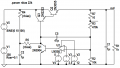
I'd like to ask for advice about this design I put together, trying to follow the basic linear regulator topology.
V3 will be a voltage reference. Like LM336, maybe TL431, etc.
The power pass transistor (Q2) will be changed for a high voltage transistor.
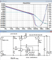
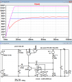
Simulation shows good behaviour. The feedback loop is stable, with plenty phase/gain margin.

Is there anything wrong in this design?

Thank you.
 

Attachments

Daniel Sala

Joined May 28, 2015
65
Hi,

Without doing some sums and simulating it, I wouldn't like to comment.

I have a chicken or the egg question, 'though: Where does the supply voltage for V2 and V3 come from? :)
 

Thread Starter

Elerion

Joined Sep 11, 2017
125
As I said, V3 will be a voltage reference. Like LM336, maybe TL431, etc.
V2 will come from a low voltage secondary winding, and stabilized. That portion of the circuit is easy for me, that is why I left it out.

Attached, ltspice file and opamp model.
 

Attachments

crutschow

Joined Mar 14, 2008
34,281
The regulator appears to become unstable at lower output voltages.
What is the minimum output voltage you will need?
You may need to significantly increase the value of C5 to maintain stability.

Note: Do the simulation with the initial operating point skipped (below), to see the initial startup oscillations.

upload_2019-5-22_11-55-31.png
 
Last edited:
None of your transistors are rated high enough for the voltage indicated by your design.
Q2 is a power transistor but is only rated at 60 volts, collector to emitter. The 2N2222 is only rated at 30 volts.
 

Thread Starter

Elerion

Joined Sep 11, 2017
125
Note: Do the simulation with the initial operating point skipped (below), to see the initial startup oscillations.
Thanks for that one. Didn't know.

You may need to significantly increase the value of C5 to maintain stability.
It seemed to me that it was stable enough: 16 dB gain margin, 83º phase margin. Or did I make a mistake in the setup?
 

Attachments

crutschow

Joined Mar 14, 2008
34,281
It seemed to me that it was stable enough: 16 dB gain margin, 83º phase margin. Or did I make a mistake in the setup?
No.
But at lower output voltages the gain/phase margin goes down and the circuit can oscillate (below).

What is the minimum output voltage setting you want?

upload_2019-5-22_13-13-49.png
 

Thread Starter

Elerion

Joined Sep 11, 2017
125
But at lower output voltages the gain/phase margin goes down and the circuit can oscillate
Interesting... nevertheless, I ran the loop gain simulation with the feedback resistors set for low enough output voltage (so I get the oscillations in trans, as you suggested).
Sure, gain margin drops from 17.8 dB (high output voltage) to 16.3 dB (low output voltage).
The margin is smaller for lower output voltage (as you said), but still is plenty.

Isn't it possible to test the loop gain for any voltage?
This test is important for me, because it is the way I was planning to test the prototype's stability (using an injection transformer), because otherway, it is very hard to know that the supply will be stable for any load and output voltage.

What is the minimum output voltage setting you want?
80 V
 

crutschow

Joined Mar 14, 2008
34,281
Isn't it possible to test the loop gain for any voltage?
The worst-case is the lowest voltage.
You can use the .step param X function to step voltages and resistances to check at various output voltages and loads.
Also could step C5 to see the change with compensation capacitor value.

For example, below is the Bode plot for two values of R3 (output voltage).
(Note that R7 is not needed, since a voltage source is a short (has zero impedance).

upload_2019-5-22_13-49-7.png
 

Thread Starter

Elerion

Joined Sep 11, 2017
125
For example, below is the Bode plot for two values of R3 (output voltage).
Didn't you forget to plot v(out)/v(x) ?
(x is how I labeled the node at the other side of the AC source).

I re-plot the loop gain for several resistor values as you suggested. Gain margin drops for lower voltages, but the difference is very small.

Now, to get more interesting... if we use a 470 pF compensation cap, the gain margin gets 35 dB even for low voltages (which is a very good margin), still I get oscillations in trans simulation for low output voltages. Attached.

Even though it seems to not be oscillating very much (red trace in trans plot), the voltage at Q1 collector is swinging like mad :)

There must be something wrong somewhere...
 

Attachments

Thread Starter

Elerion

Joined Sep 11, 2017
125
That doesn't change the curve shape, just the reference level.
Yes, I see that.
Try connecting a 10nF cap between the base and collector of Q1.
I didn't feel comfortable with the circuit. I was looking for a regulator which can be determined to be stable by measuring the loop gain, and I'd rather avoid patching (adding some capacitance here, some there... trial and error).

So I removed the opamp, and used a simple mosfet as an amplifier and also voltage reference. Obviously, the regulation is not perfect, but for my purpose (I'll fine adjust it), good enough. Now the gain is much lower, and I cannot seem to be able to make it oscillate.
I built it, and it works. I also measure the loop gain, and it has plenty of phase and gain margin.

Anything wrong with it? Something I could have missed and could be be improved?

I suppose your circuit follows a similar approach, though it seems more complex to me (you use a voltage refence, and depletion mosfet. Why?).
Why R4 so small?
Why the current limitting circuit for U2?
 

Attachments

crutschow

Joined Mar 14, 2008
34,281
you use a voltage refence, and depletion mosfet. Why?
Your circuit uses the threshold voltage of the MOSFET as the reference voltage for the output voltage setting.
This voltage varies significantly between different MOSFETs, even of the same part number, (often a factor to 2:1 or more) and that voltage is temperature sensitive, so it makes a poor reference for a voltage regulator circuit.
That's why Bordodynov used a voltage reference for that purpose.
You should too.
Why the current limitting circuit for U2?
It limits the output current.
 
Last edited:

Bordodynov

Joined May 20, 2015
3,177
I used this type of transistors, which allow to realize some requirements.
The transistor above the reference voltage source increases the operating voltage of the reference voltage source. The top transistor of this type allows you to remove the pull-up resistor to the input power source. This increases the stabilization factor and reduces output pulsations.
I made an output current limit. If this is not necessary, you can throw one transistor and a resistor. This will simplify the scheme.
 

Bordodynov

Joined May 20, 2015
3,177
I have a pulsation on the output on the diagram. Peak-to-peak is about 0.1 mV (pulsation at the input is 20 V), f, which means that the ripple suppression factor is 200,000. This is the result of using transistors with a built-in channel.
 
Top