High Voltage Buck Converter

Thread Starter

gdylp2004

Joined Dec 2, 2011
101
Hi guys,

I'm new in here and hope I could get some advices.

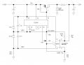
I am designing a 100V-28V DC-DC Buck converter but has encountered a problem when choosing a suitable high-frequency switch. As suggested by many designers online, pMOS is preferred for Buck operation. However one big issue is the limitation of the Vgs (typ: +-20V) which I believe is the reason why I could not utilize this as what other designers usually do.

As seen in the attached schematic, in order to turn off the pMOS switch, Vg must not be lower than both Vs and Vd by the threshold voltage indicated by the manufacturer. That is, |Vgs|< |Vth| & |Vgd| < |Vth|. Since Vs is always 100V (because source is tied to +ve terminal of battery) and Vd = 28V (assuming the capacitor is large enough to hold the charge, hence o/p voltage well) and assuming the Vth is -4V, is it correct that to turn switch off, Vg must be > Vs-|Vth| and also Vg > Vd-|Vth| since a pure MOSFET drain and source is interchangeable.

If this is true, a typical pMOS with only Vgs max of 20V could not handle since we must ramp up Vg all the way to 96V and above (for my case) but that also implies the potential difference between Vg and Vd is 68V which is > 20V and thus the FET will breakdown.

And if everything I've explained is true, is there a way to overcome this? TIA.
 

Attachments

jimkeith

Joined Oct 26, 2011
540
Yes, your analysis is correct--this is the standard problem in high-side switches--at least with a P-Channel device, a negative voltage (Vgs) will turn it on and a 12V zener (with proper current limiting) will protect it from damage--on the other hand, an N-Channel device requires a boot-strapped or other voltage source that is above the supply voltage.
 

Thread Starter

gdylp2004

Joined Dec 2, 2011
101
Hi Jim,

Thanks for your reply. If I would like to insist to use a pMOS instead, how would the Zener diode protects the MOSFET from damaging, according to my knowledge a Zener has a property of maintaining a constant 12V (in this case) under reverse biased condition right? If true, should I connect the Zener across the drain and gate to clip the potential at 12V?

TIA.
 

SgtWookie

Joined Jul 17, 2007
22,230
The gate voltage is always specified with reference to the source terminal as Vgs. Therefore, the Zener needs to be connected between the gate and the source terminals.
 

Thread Starter

gdylp2004

Joined Dec 2, 2011
101
The gate voltage is always specified with reference to the source terminal as Vgs. Therefore, the Zener needs to be connected between the gate and the source terminals.
Hi SgtWookie,

Thanks for your reply.

Assuming my source (Vs) and drain voltage (Vd) is always held constant at 100V and 28V respectively, and also assume the pMOS has a threshold voltage of a typical value of -4V. In order to cut off the switch totally, we knew Vg (gate voltage) must be at least > 96V since criteria for MOSFET to operate in the cutoff region is |Vgs| < |Vth|.

And in this particular case, assuming I've set Vg = 100V so that Vgs would be 0 and Vg is so much higher than Vd (about 100-28=72V), therefore both side would not be conducting and hence pMOS operate into the cut-off region. Now, this 72V across the gate and drain is my biggest concern because the manufacturer stated max Vgs = 20V, and since a MOSFET drain and source is interchangeable, therefore I should also assume that the max Vgs also implies the max of Vgd? And if true, shouldn't the Zener diode should protect the potential between gate and drain instead of gate and source?

TIA.
 

jimkeith

Joined Oct 26, 2011
540
Try this circuit on for size--the 78S40 regulator sits 10V below the incoming bus and is in good position to drive the P-Channel MOSFET--the feedback is translated by an attenuating differential amplifier--the internal op amp is of little use here as it is rated for only 5V.

The spec sheet describes how to drive a PNP transistor.
http://www.national.com/ds/LM/LM78S40.pdf

At this point, it is untested--let me know how it works out.
 

Attachments

Last edited:

Thread Starter

gdylp2004

Joined Dec 2, 2011
101
Try this circuit on for size--the 78S40 regulator sits 10V below the incoming bus and is in good position to drive the P-Channel MOSFET--the feedback is translated by an attenuating differential amplifier--the internal op amp is of little use here as it is rated for only 5V.

The spec sheet describes how to drive a PNP transistor.
http://www.national.com/ds/LM/LM78S40.pdf

At this point, it is untested--let me know how it works out.
Thanks Jim,

The following is my strategy which I hope you could give some pointers first.

The general circuit would be as what I've attached in my maiden post. However I am using IR2117(http://www.farnell.com/datasheets/59982.pdf) to drive the high-side MOSFET by adopting the bootstrap configuration. My steps are followed closely to this guide (http://www.irf.com/technical-info/appnotes/an-978.pdf) which unfortunately seems like an old technology as it is published in 2007.

My selected and only High-side MOSFET would be IRF540 (http://www.irf.com/product-info/datasheets/data/auirf540z.pdf) 100V nMOS with ultra-low ON resistance, hence reducing power loss during switching. Moreover it is packaged in the TO-220 style for easier mounting option for me since I'm building this Buck on breadboard.

Tentatively, this is an open-loop system and I'll incorporate feedback features to adjust the duty ratio (D) of the system for any load change in the future.

What do you think of my design?

Thanks in advance (TIA).

PS: I've added a link to a report which a group of engineering students have done similar Buck circuit as compared to my requirement.
 
Last edited:

SgtWookie

Joined Jul 17, 2007
22,230
Assuming my source (Vs) and drain voltage (Vd) is always held constant at 100V and 28V respectively, and also assume the pMOS has a threshold voltage of a typical value of -4V. In order to cut off the switch totally, we knew Vg (gate voltage) must be at least > 96V since criteria for MOSFET to operate in the cutoff region is |Vgs| < |Vth|.
First, the voltage at the drain will vary over a wide range, from nearly 100v when the MOSFET is on, to negative voltage when the diode is conducting.

Second, you need to stop thinking in terms of the gate voltage referenced to ground, as you will wind up frying many, many MOSFETs.

You need to think in terms of Vgs, as that is the only thing that 'matters' to the MOSFET. If Vgs exceeds ±20v (15v for some MOSFETs) you will destroy it.

Third, the threshold voltage should be considered only when attempting to determine where the MOSFET will be considered turned OFF. Many people new to MOSFETs use Vgs(th) in an attempt to determine when the MOSFET is ON. You need to look at the Rds(on) specification for that; it will give you the resistance at (a) specific Vgs(es)

And in this particular case, assuming I've set Vg = 100V so that Vgs would be 0 and Vg is so much higher than Vd (about 100-28=72V), therefore both side would not be conducting and hence pMOS operate into the cut-off region. Now, this 72V across the gate and drain is my biggest concern because the manufacturer stated max Vgs = 20V, and since a MOSFET drain and source is interchangeable, therefore I should also assume that the max Vgs also implies the max of Vgd?
No. Vdss is the maximum voltage from drain to source, and max Vgs is specified separately.

If you fail to consider the MOSFET body diode, you'll have a surprise if you connect it backwards.

And if true, shouldn't the Zener diode should protect the potential between gate and drain instead of gate and source?
If the drain of a P-ch MOSFET is more positive than the drain by ~0.7v, the body diode will conduct.

I'll repeat; think Vgs, not Vg.
 
Last edited:

SgtWookie

Joined Jul 17, 2007
22,230
Try this circuit on for size--the 78S40 regulator sits 10V below the incoming bus and is in good position to drive the P-Channel MOSFET--the feedback is translated by an attenuating differential amplifier--the internal op amp is of little use here as it is rated for only 5V.

The spec sheet describes how to drive a PNP transistor.
http://www.national.com/ds/LM/LM78S40.pdf

At this point, it is untested--let me know how it works out.
Hi Jim,
Most of it looks reasonable, except I have my doubts about the 10k pull-up for the MOSFET gate. If the gate charge is very significant (and I'll bet it will be, due to the necessary Vdss and Id ratings) it will cause slow turn-off of the MOSFET, and resulting high power dissipation in the MOSFET.

[eta]
You might consider using a relatively simple gate driver; something like the one attached.

[eta]
Updated schematic & simulation to compare using just a 10k pullup vs the driver.
Just for some quick specs, the MOSFET used in the simulation: Rds(on)=45m, Vdss=-30, Qg=36nC
The frequency is 10kHz, duty cycle is 3%.
I forgot to show power dissipation in the MOSFETs for the comparison, but M2 dissipation average exceeds 12.5W, where M1's dissipation is ~220mW. That is a 99.98% reduction in the MOSFET power dissipation.
 

Attachments

Last edited:

jimkeith

Joined Oct 26, 2011
540
Hi Jim,
Most of it looks reasonable, except I have my doubts about the 10k pull-up for the MOSFET gate. If the gate charge is very significant (and I'll bet it will be, due to the necessary Vdss and Id ratings) it will cause slow turn-off of the MOSFET, and resulting high power dissipation in the MOSFET.
Yeah, I had my doubts about that detail--thanks for the suggestion.

If you are going to use the IR2117 driver, go to a higher voltage and lower Rdson N-Channel MOSFET too.

Also open loop is a poor way to go--way too many variables to predict output voltage.
 

SgtWookie

Joined Jul 17, 2007
22,230
<snip>My selected and only High-side MOSFET would be IRF540 (http://www.irf.com/product-info/datasheets/data/auirf540z.pdf) 100V nMOS with ultra-low ON resistance, hence reducing power loss during switching.
You have a 100v supply, and when the MOSFET is off and the inductor is discharging, you will have exceeded the Vdss rating of the MOSFET by at least the Vf of the diode.

Select a MOSFET that has a Vdss of 125v or higher (100v/80%)

Moreover it is packaged in the TO-220 style for easier mounting option for me since I'm building this Buck on breadboard.
1) Solderless breadboards are not designed to have TO-220 packaged ICs jammed into their sockets. You will damage the sockets at that position, making the connections very "dicey" for later projects.

2) Solderless breadboards won't take much current, and have a lot of parasitic L, C and R. They are best used for low frequency analog or digital circuits. Even though your buck might only be 50kHz or so, you are trying to drive the gate with a square wave; and an ideal square wave is composed of the fundamental frequency plus ALL of the odd harmonics of that frequency. This implies unlimited bandwidth. Since that is not quite possible, your square wave will not be a perfect square wave. If you build it on a breadboard, it will be very far from a perfect square wave; more like a snake in a hurry.

Use stripboard or veroboard or prototype board. Keep your wiring as short as possible to minimize parasitics. Decide on your layout before you try to wire it up.

Tentatively, this is an open-loop system and I'll incorporate feedback features to adjust the duty ratio (D) of the system for any load change in the future.
Don't go open-loop. Just for starters, you will overshoot your target output voltage by a very large margin on start-up. If your load changes any significant amount, so will your output voltage.
 

Thread Starter

gdylp2004

Joined Dec 2, 2011
101
You have a 100v supply, and when the MOSFET is off and the inductor is discharging, you will have exceeded the Vdss rating of the MOSFET by at least the Vf of the diode.

Select a MOSFET that has a Vdss of 125v or higher (100v/80%)
That sparks another question from me. When the MOSFET is off, hence the diode (which I've selected: http://www.st.com/internet/com/TECHNICAL_RESOURCES/TECHNICAL_LITERATURE/DATASHEET/CD00003323.pdf) is conducting. It has a max. of Vf = 820mV and the anode connected directly to GND, which in turn pulls the MOSFET source voltage to 0-0.82V = -0.82V which will give problem to my IR2117 driver.

As what recommended in Figure 27 of page 25 in this guide (http://www.ti.com/lit/ml/slup169/slup169.pdf), a zener diode connected between Vs PIN of the driver and GND would stop the voltage at the Vs PIN to fall further than the Vf of the zener diode. And since during MOSFET = OFF, the voltage across my schottky diode and the zener would be different, therefore a Rgate as shown in Figure 27 would handle this potential difference.

However one setback for this Rgate would be it constitute to a longer charging time constant since the charging current path of the bootstrap capacitor would be from starting from Vcc -> Bootstrap diode -> bootstrap capacitor -> split into two paths 1) Rgate -> Schottky diode -> GND & 2) Zener diode -> GND.

If my switching Freq = 100kHz, that is my period, T = 10μs. Duty ratio for me, D = Vin/Vout = 28/100 = 0.28. Hence Toff = 0.72 X 10μs = 7.2μs which should be sufficient to charge my bootstrap cap after including all the propagation delays, rise/fall times?

In most of the guides, there is more or less a standard formula to obtain the min. capacitance rating for the bootstrap cap by using the following values:

Qg = Gate charge of high-side FET​


f = frequency of operation

ICbs (leak) = bootstrap capacitor leakage current​

Iqbs (max) = Maximum VBS quiescent current

VCC = Logic section voltage source

Vf = Forward voltage drop across the bootstrap diode


VLS = Voltage drop across the low-side FET or load​


VMin = Minimum voltage between VB and VS.

Qls = level shift charge required per cycle (typically 5 nC for 500 V/600 V MGDs and 20 nC for1200 V MGDs)

Im pretty fine with most of the parameters except for Iqbs, Vmin and Qls. Can anybody suggest how do I go about with these parameters?​

Thanks.​
 

Thread Starter

gdylp2004

Joined Dec 2, 2011
101
I think I've made a mistake, I should add schottky instead of a zener. However that brings up another question which is, I am suppose to choose the lowest Vf(max) ratings of this diode so as to pull up voltage at Vs as close to COM as possible, but if there is such a diode exists, I could also replace with my freewheeling diode with this? And hence at high-side switch OFF instances, the voltage at the source of the MOSFET = Vs at the Vs PIN of the driver and that would not solve any problem? Thanks.
 

Thread Starter

gdylp2004

Joined Dec 2, 2011
101
Anybody here think that I could replace the traditional gate driver with optocoupler? But it seems that the typical falling and rising time is always in the order of miliseconds and not micro or lesser. Is that the primary reason why optocoupler is not being utlised for buck converter drivers till today?
 

T.Jackson

Joined Nov 22, 2011
328
Try this circuit on for size--the 78S40 regulator sits 10V below the incoming bus and is in good position to drive the P-Channel MOSFET--the feedback is translated by an attenuating differential amplifier--the internal op amp is of little use here as it is rated for only 5V.

The spec sheet describes how to drive a PNP transistor.
http://www.national.com/ds/LM/LM78S40.pdf

At this point, it is untested--let me know how it works out.
Is it just me, or does this looks dangerous?


SgtWookie

Joined Jul 17, 2007
22,230
Optocouplers are generally pretty slow.

There are some fairly recent optocoupler gate drivers that have improved specifications.

There is a newer technology, called "digital isolators". Try Googling "digital isolator gate driver".
These are basically capacitively coupling logic signals to achieve HV isolation. It's far faster than using optocouplers.
 

jimkeith

Joined Oct 26, 2011
540
Is it just me, or does this looks dangerous?
What looks dangerous about it?
SgtWookie already indicated that the 10K resistive pull-up is too weak and suggested a totem-pole driver stage. If this is incorporated, I believe that it is a viable candidate. There may also be a few other nuances that need to be cleaned up. The 78S40 driver is a great chip--I have used it in numerous applications.
 
Top