I hate to ask but I feel like I am going around in circles. This is my first time messing with a PNP mosfet.
Lets say I am looking to turn a resistive load on and off. Using PNP because like in many automotive applications I do not have the ability to control ground side.
For a hypothetical situation, lets say 12V, 15A. Driving with a gate voltage of 10V. Steady state, as demand could be to be on for 2 seconds or 30 minutes.
I randomly see this Vishay Si4497DY.
Vds=30V, continuous drain current rating of 19-36A depending on how you look at it. "Pulsed" drain current up to 70A.

Looking at Rds:
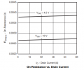
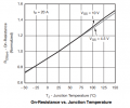
Rds@25C=~0.0027 ohm, then using the normalized curve when its hot its 0.0027*1.5=0.00405 ohm.
P=I^2*V, I get 15*15*0.0405=0.911W..
Looking at Rth:

If i use the Rth from the table, for <10s and Rth of 35, then the temp rise will be:
Trise=0.911*35=32 deg C, for a Thot=57 deg C.
If I use Rth from the note C, its "maximum under steady state" is 80C/W
Trise=0.911*80= 73C which is Thot of 98C.
So normally at this point I would think I am well in the good. For worst case condition of Rds and Rth it still does not go over 150 Deg C, or even near it...
BUT... Then I notice this pesky Safe Operating Area chart. Note, I added the red and blue lines..
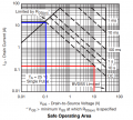
If I go to the Vds of 10V, using the red line and go up to the DC operating line, then over to the vertical axis, I end up at like 0.16A?? Does this mean that if I have 12V on the source, my load on the drain, and the other end attached to ground, now this MOSFET can only supply 0.16A??? This does not seem right.
On the flip side, if I say OK what is the voltage this MOSFET can take at 15A, using the blue lines that puts me down at just over 0.1Vds??
I must be interpreting this incorrectly as the only place there is a CONTINUOUS drain current mentioned above of 20A is in the pulsed regions??
Anyone able to help set me straight here?
Many thanks in advance!
Lets say I am looking to turn a resistive load on and off. Using PNP because like in many automotive applications I do not have the ability to control ground side.
For a hypothetical situation, lets say 12V, 15A. Driving with a gate voltage of 10V. Steady state, as demand could be to be on for 2 seconds or 30 minutes.
I randomly see this Vishay Si4497DY.
Vds=30V, continuous drain current rating of 19-36A depending on how you look at it. "Pulsed" drain current up to 70A.

Looking at Rds:


Rds@25C=~0.0027 ohm, then using the normalized curve when its hot its 0.0027*1.5=0.00405 ohm.
P=I^2*V, I get 15*15*0.0405=0.911W..
Looking at Rth:

If i use the Rth from the table, for <10s and Rth of 35, then the temp rise will be:
Trise=0.911*35=32 deg C, for a Thot=57 deg C.
If I use Rth from the note C, its "maximum under steady state" is 80C/W
Trise=0.911*80= 73C which is Thot of 98C.
So normally at this point I would think I am well in the good. For worst case condition of Rds and Rth it still does not go over 150 Deg C, or even near it...
BUT... Then I notice this pesky Safe Operating Area chart. Note, I added the red and blue lines..

If I go to the Vds of 10V, using the red line and go up to the DC operating line, then over to the vertical axis, I end up at like 0.16A?? Does this mean that if I have 12V on the source, my load on the drain, and the other end attached to ground, now this MOSFET can only supply 0.16A??? This does not seem right.
On the flip side, if I say OK what is the voltage this MOSFET can take at 15A, using the blue lines that puts me down at just over 0.1Vds??
I must be interpreting this incorrectly as the only place there is a CONTINUOUS drain current mentioned above of 20A is in the pulsed regions??
Anyone able to help set me straight here?
Many thanks in advance!
Attachments
-
20.9 KB Views: 2

 Facebook
 Google
 GitHub
 Linkedin

