help with 555 TIMER - variable frequency and variable duty cycle

Thread Starter

minkey01

Joined Jul 23, 2014
185
Hi.

I'm trying to design a 555 timer circuit powered by +12V and outputs +5V pulses with variable frequency and variable duty cycle.

It should have :

Clock Range Switch : x1 or x10 setting
Clock Rate Knob : 0.1 Hz - 10 Hz (x1)
1 Hz - 100 Hz (x10)
Duty Cycle Knob : 10% -90%

The duty cycle range can be wider if possible. Those % values above are just the bare minimum.

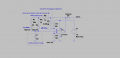
Here is a picture of how far I got. Not sure if this is right or getting close. Could someone please help me with the values and needed new components?

Thanks so much! Happy Holidays!

555 clock.jpg
 

Thread Starter

minkey01

Joined Jul 23, 2014
185
Found this circuit too. Maybe this is a better starting point. It is suppose to be independent variable frequency and duty cycle.

Thoughts?

Does anyone have a LTSpice model for the LM393? I would like to try to simulate this latest circuit.

555 clock 3.jpg
 

Thread Starter

minkey01

Joined Jul 23, 2014
185
Who ever drew that should be taken outside and have unpleasant things done to them.

One is the square wave output form the 555, the other is result of the comparison of the triangle wave and the input from the pot (R5).


The orange line (DCV) would be the voltage u2a pin 5.
The green line (triangle) is the input at u2a pin 6.
The red line is the ouput at u2a pin 7.

Not shown on this graph is the output from the 555 pin 3.
Ok, thank you. So I only would be using pin 7 output. Is there anything else wrong with the circuit? Still trying to find a LM393 LtSpice model, so I can tune to my values.
 

dannyf

Joined Sep 13, 2015
2,197
Just so you know, the 555 can be replaced by that unused comparator. The design is a little bone headed in that regard.
 

dannyf

Joined Sep 13, 2015
2,197
here is a simple demo, showing how the whole thing can be fitted to one dual opamp/comparator.

comparator pwm generator.PNG

U1 acts like an oscillator, producing square wave output. On the comparator, it produces a ramp - shown as the blue trace.

U2 is a simple comparator. By adjusting the pot (R2+R3), you control the duty cycle.

Fairly easy to construct. Values are not critical.
 

Thread Starter

minkey01

Joined Jul 23, 2014
185
here is a simple demo, showing how the whole thing can be fitted to one dual opamp/comparator.

View attachment 116588

U1 acts like an oscillator, producing square wave output. On the comparator, it produces a ramp - shown as the blue trace.

U2 is a simple comparator. By adjusting the pot (R2+R3), you control the duty cycle.

Fairly easy to construct. Values are not critical.
Hi, Danny. A few questions:

1) What is the value of C2? It is cut off in the picture.
2) How would I change the frequency?

Thanks! This really looks great.
 

Plamen

Joined Mar 29, 2015
101
555 has inherently asymmetrical rise/fall time because of different charge/discharge paths and in most cases it is hard to adjust by one pot the duty cycle on either side of 50%. A simple OP AMP circuit can adjust both frequency and duty cycle. The duty cycle adjustment pot is shown as 99k and 1k resistors. Range selection by cap, frequency adjustment by R2. A MOSFET is shown as level shifter to make 5V amplitude.
The cap could also be referred to virtual ground (10k mid point). Unipolar 12V power supply is shown - hence the 10k/10k divider to make "virtual ground"
upload_2016-12-9_10-25-42.png

Even more advance options present the LTC699X Timer Blox chips from Linear Technology.
LTC6990 is a voltage controlled oscillator; LTC6991 a low frequency clock. Download from LT web site the TimerBlox Excel based design tool.
http://www.linear.com/products/timerblox (under SW and simulation)
Pick a timing function, plug your requirements, click and get specific example.
These chips have very accurate timing (1%) without caps. They have course adjustment by ratio of resistors and fine adjustment by a resistor value. There is a PWM member in the timer blox family too (LTC6992). Download LTSpice (free) and design with gusto.
upload_2016-12-9_10-35-21.png
 

Attachments

crutschow

Joined Mar 14, 2008
34,281
Here's my take on a three opamp circuit using one LM324 package.

U1 is configured as a comparator that generates a square-wave.

This is converted to a triangle-wave by U2, configured as an integrator.

U3 is configured as another comparator, which compares the triangle-wave voltage with the voltage from pot U4 to generate the PWM signal with duty cycle of 0% to 100% by adjusting U4.

The frequency goes from about 0.1Hz to 11Hz with C1 = 3.3uF by adjusting U5.
If C1 is switched to a value of 0.33uF then the frequency range will be about 10Hz to 110Hz.

upload_2016-12-9_16-19-11.png
 

Attachments

Bordodynov

Joined May 20, 2015
3,177
Thank you.
Now I will make a new symbol lm324.sym. I will add this symbol in my library. After that I will be able to use your circuits that use lm324.
 
Top