Facebook
 Google
 GitHub
 Linkedin
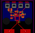
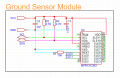
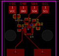
I designed this capacitive moisture sensor, I'm not sure if it will work. I'm posting it here to see if anyone can find anything I should fix before I order the PCB (I'm a student, I don't have a lot of money to waste so I'd like to catch errors before I spend the money).
Attachments
-
 69 KB Views: 41
 -
 15 KB Views: 42
 -
 42.7 KB Views: 32