Help! Cycle bike circut board medium transistor

Thread Starter

Lucypotomus

Joined Jun 11, 2022
5
Hi all,

Super newbie here! I have been dabbling in electronics repair, circuit board repair, and coding for only a short time.

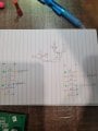
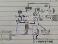
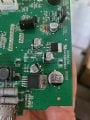
I recently bought a used Echelon connect Cycle bike that worked but only for a short time (not under warranty). I thought I could fix it no problem, did some troubleshooting, got a new motor, but still no. I turned my attention to the circuit board which is where I found the burnt medium transistor (first photo). The full identification on this bad boy is utcrltf 2sd882l.

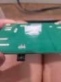
I found a SD882 Trans NPN 30v 3A SOT32 from Digikey and ordered it. I took out the old transistor and soldered in the new one. Plugged everything back in and the transistor slowly started getting hot and I could smell it. I turned it off, there doesn't seem to be damage to the new transistor but I think if I left it on there would have been. I did hear the beep and saw the light that turns on on the bike console so some parts are working. I have more photos of my work with the new transistor, my only thought is maybe I should have cleaned the old burn spots better?

This is the extent of my knowledge, I have no idea how to troubleshoot past this point. Any ideas? Am I way out of my league here?

Thanks in advance!
 

Attachments

dl324

Joined Mar 30, 2015
16,846
Welcome to AAC!
This is the extent of my knowledge, I have no idea how to troubleshoot past this point. Any ideas? Am I way out of my league here?
If the original problem was a transistor that went bad, replacing it would fix the problem. If the real problem was something up- or downstream caused it to fail, then replacing the transistor wouldn't fix the problem.

Are you able to trace the circuitry around the transistor and create a schematic? Do you have a DVM?

You have too much solder on the transistor leads. If it isn't no lead solder, the joints are cold.
 

sagor

Joined Mar 10, 2019
903
Agree that the solder join may be "cold". In the top picture, there does not seem to be any solder flowing through the holes where the legs are. With relatively normal solder flow, there should be solder on the legs visible from both sides..
 

Alec_t

Joined Sep 17, 2013
14,280
The photo is a bit blurred, and it may be a trick of the light, but the connections of the U1 IC legs look a bit suspect and ZD1 looks a bit cooked?
 

Thread Starter

Lucypotomus

Joined Jun 11, 2022
5
Welcome to AAC!
If the original problem was a transistor that went bad, replacing it would fix the problem. If the real problem was something up- or downstream caused it to fail, then replacing the transistor wouldn't fix the problem.

Are you able to trace the circuitry around the transistor and create a schematic? Do you have a DVM?

You have too much solder on the transistor leads. If it isn't no lead solder, the joints are cold.
Thank you so so much! Since the transistor was already getting hot after seconds of being turned on, the problem must be elsewhere. I have a DVM so I can mess around with that to see if I come up with anything.

I also definitely need to find my better solder iron or buy a new one and fix up those leads.
 

dl324

Joined Mar 30, 2015
16,846
I have a DVM so I can mess around with that to see if I come up with anything.
We need a partial schematic so we can give better suggestions regarding what nodes to probe. The terminals on the transistor would be a start, but that's not likely to give sufficient information for troubleshooting.
 

Thread Starter

Lucypotomus

Joined Jun 11, 2022
5
We need a partial schematic so we can give better suggestions regarding what nodes to probe. The terminals on the transistor would be a start, but that's not likely to give sufficient information for troubleshooting.
I have never reverse engineered a schematic before and also don't know which way is up at this point so please forgive my ignorance.

I color coded the contact points and separated it between which contact point had negative and positive.

I honestly don't know which direction is upstream or downstream- but based on the location of the power supply input I think U2 is upstream going down to Q1 and then to C21. It looks like Q1 also goes to C4.

The volts don't make any sense to me which is why I did it both ways (+ and -).

I also used the continuity function and found OL on all except the ones I labeled "continuity" as I got a beep on those guys.

What this means? I don't know, I'm very lost.
 

Attachments

dl324

Joined Mar 30, 2015
16,846
I have never reverse engineered a schematic before and also don't know which way is up at this point so please forgive my ignorance.
That's fine. We can ask for any details that aren't clear.

Try to take a picture with no glare so we can see traces better. If possible, use a small aperture size (large f-stop number) so things will be in better focus.

You don't need to draw the traces. Just "wires" connecting them like this:
sch2.jpg
The horizontal line on the left is the base (marked B below), the terminal with the arrow is the emitter (marked E below), the other terminal is the collector (marked C below). Use your ohmmeter to verify connections to other components. The capacitor connections aren't helpful at this point.

Read and post the markings on the integrated circuits. U2 might be a voltage regulator. Q2 and Q2 are transistors, but we don't know type (MOSFET or BJT) and polarity (N or P type).

Clipped and rotated images:
sch1.jpgclip1.jpg
 

Dodgydave

Joined Jun 22, 2012
11,285
From post #4, what is the voltage on the Collector ( middle pin) and Emitter , and what is the name on U5 chip that looks like a switchmode regulator.?
 
Last edited:

Thread Starter

Lucypotomus

Joined Jun 11, 2022
5
Read and post the markings on the integrated circuits. U2 might be a voltage regulator. Q2 and Q2 are transistors, but we don't know type (MOSFET or BJT) and polarity (N or P type).
Ok, I think this will give more information. New drawing and better photo. Here is what I found out about the components;
Q1=2SD882=NPN Medium transistor
U2=7133 7S18GA=voltage regulator
Q2=M6=PNP transistor
Q3=L6=NPN transistor
U1=UTC LD1117AG 33A 81VDT8=voltage regulator?
U5=XL2576S ADJE1= DC DC converter

I used the ohmeter (20k) from the legs of Q1 to the leads from where I think power comes from (labeled A1-A3 and B1-B9)
These are the results
B-B1 20 then says 0.L
B-B2 0.L
E-B1 0.L
E-B2 0.L
C-B1 5.9
C-B2 6.18
B-A2 10.74
E-A2 14.61
C-A2 15.98
B-B4 0.L
B-B5 18.4
B-B6 0.L
B-B7 12.11
C-B4 10.88
C-B5 6.2
C-B6 12.28
C-B7 1.01
E-B4 0.L
E-B5 0.L
E-B6 0.L
E-B7 13.61
 

Attachments

Top