Good heat but poor electrical conductor

Thread Starter

gdylp2004

Joined Dec 2, 2011
101
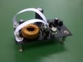
Nothing fishy over here. The hardware you saw is definitely not the final product that will be fitted in the structure of the satelitte. It'll be improved after a few versions and decided if it is fit for flight.

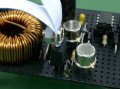
The reason why I would want to dissipate heat away from the hottest element to the posts is to actually make a point that unwanted heat can be dumped to the casing, (currently the posts). And if I can show that the posts' temp increases while the temp in the MOSFET decreases, because of some method of heat dissipation (like the idea in my first post), I could proved that this method would most probably work for the final product as well.

Regarding the use of MOSFET instead of an old fashion PNP, I've read it from somewhere else that a PNP BJT is not as good as a MOSFET if I am switching at 100kHz.
 

Thread Starter

gdylp2004

Joined Dec 2, 2011
101
Update:

I've cut out strips of paper to mimic the copper strips as intended from my first post. What's only missing here is the thermal pad I'll only insert between the heat source and the strips when the real sopper strips are used.

Please see attached and comment. I wonder if this method is worth trying.
 

Attachments

MrChips

Joined Oct 2, 2009
34,866
If someone had asked me if I could design a terrestrial based SMPS, I would have to reply, "maybe". If they said it has to function in space, I would definitely say, "Count me out!"
 

THE_RB

Joined Feb 11, 2008
5,438
1. Thanks for posting the schematic. At 3A and maybe 30% duty, with a modern FET, I still can't see why your FET will get to 130 degrees!

2. Putting bendy copper strips from a vertical TO220 to a post 2" away is just plain nuts. They will radiate more than conduct, and the post won't be a good conductor lengthwise anyway.

Have you looked inside any commercial SMPS devices? It is very common to bolt the TO220 flat to the outer metal casing or plate, and bend its legs 90 degrees and they solder to the PCB which runs parallel to the case.
 

Thread Starter

gdylp2004

Joined Dec 2, 2011
101
1. Thanks for posting the schematic. At 3A and maybe 30% duty, with a modern FET, I still can't see why your FET will get to 130 degrees!
Hi Roman Black (RB),

Off topic a little, I might know why the MOSFET shot up to about 130°C. That could be the notorious switching loss. As seen in the newly attached scope3.jpg, it seems that the rise and falling time of the V(gs) seems a little longer than it should be. I've already chosen the smallest Q(g) but this "slow" turn on and off seems to persist. Well, I think the cause of the problem could be my gate driver which has only a 200mA/420mA driving capability.

Assuming I've replaced a more powerful gate driver now, I would expect the overshoot, ringing occured during the transition states would amplify. Reading from the internet tells me that I should add a RC snubber between the buck's main inductor and switch node, should be able to supress these transients adequately. Right?
 

Attachments

Thread Starter

gdylp2004

Joined Dec 2, 2011
101
2. Putting bendy copper strips from a vertical TO220 to a post 2" away is just plain nuts. They will radiate more than conduct, and the post won't be a good conductor lengthwise anyway.

Have you looked inside any commercial SMPS devices? It is very common to bolt the TO220 flat to the outer metal casing or plate, and bend its legs 90 degrees and they solder to the PCB which runs parallel to the case.
Regarding #2) if the copper strips could radiate out all the additional heat energy before it even reaches the posts, that would be even better. Afterall, the strips act nothing but a customised heatsink.

Yes, I've seen many MOSFETs are mounted firmly onto a big baseplate for effective heat sinking. But consider that if the tab of the TO-220 is not convenient to be pressed against the case or any part of the external structure, what should we do? Adopting the heat transferring tactic as I would like to try?
 

THE_RB

Joined Feb 11, 2008
5,438
That 'scope trace is nasty! :eek:

Yep the power FET should be placed on a metal plate. Good design practice would be to properly integrate the heat paths with the enclosure in the early stages of the design, before the enclosure and PCB are finalised.
 

John P

Joined Oct 14, 2008
2,063
Any circuit that's going to space surely ought to be designed for maximum efficiency, first because dissipating power in a vacuum is difficult, and second because you probably haven't got much electrical power to play with. If some component is heating up, the device is inefficient, by definition. I can't prove it, but I think the design can be improved so that this heat sink business (extra weight, too--very bad) can be avoided completely.
 
Top