Facebook
 Google
 GitHub
 Linkedin
Hello everyone
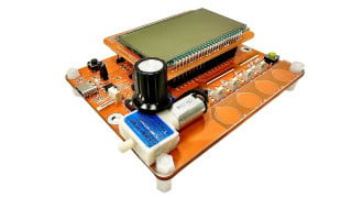
I wanted to share with you the design of a 2-layer full GNSS board that I have recently developed using Direct RF sampling architecture. The board consists of several blocks, each equipped with SMA input/output connectors, as well as an SMA connection between VCC and GND to check the noise. The board is designed to enable efficient processing of GNSS signals. The blocks are : 1. LNA , 2. 3xBGA amplifier blocks , 3. Splitter/3xBPF/Combiner, 4. Variable Gain Amplifiers (VGA). which are shown in Figures below:


One of the initial tests conducted involved checking each amplification stage using a single-tone signal at the GPS L1 center frequency of 1575.42MHz. The signal was intentionally set to a very low amplitude for testing purposes.
During the test, one notable issue arose when connecting the VCC using shielded cables to the BGA block. Even before turning on the VCC and RF , a signal was observed at the VCC SMA connection, as depicted in the following figure:

when VCC in ON / RF OFF:

Next test is in the output SMA VCC OFF/RF OFF :

RF OFF/ VCC ON:

This output makes no sense, its too much for amplifier no input its just amplified the noise, I still don't get it.
I would really like some suggestion regarding this issue.
I wanted to share with you the design of a 2-layer full GNSS board that I have recently developed using Direct RF sampling architecture. The board consists of several blocks, each equipped with SMA input/output connectors, as well as an SMA connection between VCC and GND to check the noise. The board is designed to enable efficient processing of GNSS signals. The blocks are : 1. LNA , 2. 3xBGA amplifier blocks , 3. Splitter/3xBPF/Combiner, 4. Variable Gain Amplifiers (VGA). which are shown in Figures below:
One of the initial tests conducted involved checking each amplification stage using a single-tone signal at the GPS L1 center frequency of 1575.42MHz. The signal was intentionally set to a very low amplitude for testing purposes.
During the test, one notable issue arose when connecting the VCC using shielded cables to the BGA block. Even before turning on the VCC and RF , a signal was observed at the VCC SMA connection, as depicted in the following figure:
when VCC in ON / RF OFF:
Next test is in the output SMA VCC OFF/RF OFF :
RF OFF/ VCC ON:
This output makes no sense, its too much for amplifier no input its just amplified the noise, I still don't get it.
I would really like some suggestion regarding this issue.
Attachments
-
 66.5 KB Views: 0